
 German
 Japanese
 Portuguese
 Korea
Korea
 Mexico
 Dutch
Dutch


onsemi
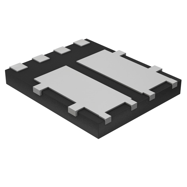
NTMFD6H852NLT1G

Why Choose Us?
Professional Platform
B2B & B2C purchasingDelivery at full speed
1-2 days deliveryWide variety
Original manufacturers365 days guarantee
Responsible quality
.png)


Tech Specifications
NTMFD6H852NLT1G Description
Tape & Reel (TR) provides mechanical support to the IC chip to ensure proper alignment and prevent damage due to vibration or shock. The FET, MOSFET Arrays that the NTMFD6H852NLT1G belongs to can be classified under the Discrete Semiconductors. NTMFD6H852NLT1G is used in a wide range of electronic devices, including computers, smartphones, televisions, cars, medical devices, and many others. NTMFD6H852NLT1G provides the computational power and functionality that enable these devices to perform their intended tasks. a vital part of the supply chain ecosystem. They convert raw materials or components into finished products, ensuring their availability for consumers or other businesses. onsemi plays a crucial role in ensuring the smooth flow of goods and meeting market demand. onsemi is responsible for ensuring the quality and safety of the products they produce. They implement quality control measures to meet industry standards and regulatory requirements. By maintaining high-quality standards, onsemi builds trust with consumers and enhances the overall reputation of their products.
FAQ
Not available to buy online? Want the lower wholesale price? Please Send RFQ to get best price, we will respond immediately


.png?x-oss-process=image/format,webp/resize,h_32)


