
onsemi
NTNUS3171PZT5G

Why Choose Us?
Professional Platform
B2B & B2C purchasingDelivery at full speed
1-2 days deliveryWide variety
Original manufacturers365 days guarantee
Responsible quality
.png)


Tech Specifications
NTNUS3171PZT5G Description
NTNUS3171PZT5G Description
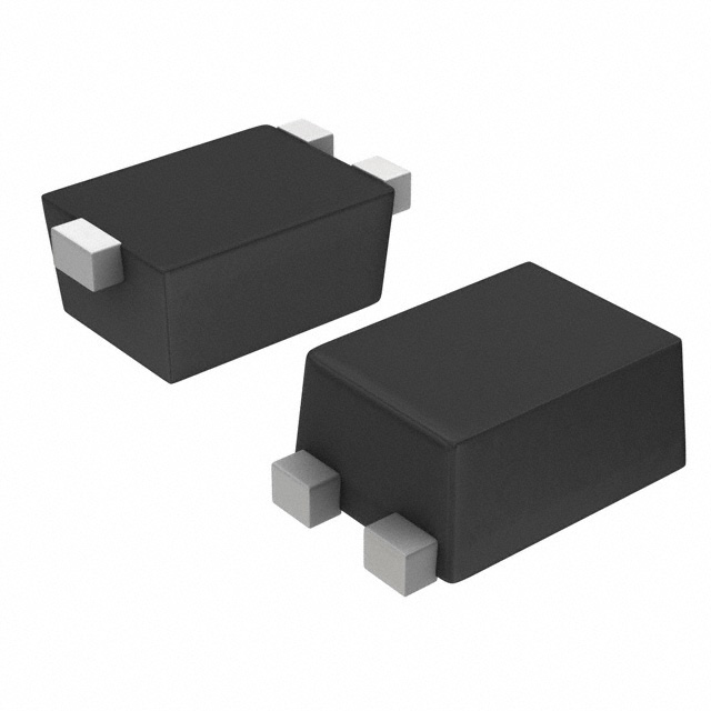
The NTNUS3171PZT5G is a MOSFET P-CH 20V 150mA SOT1123 device manufactured by onsemi. This single FET is designed for high-performance applications requiring low power dissipation and high input capacitance. With a maximum drain-to-source voltage of 20V and a continuous drain current of 150mA at 25°C, the NTNUS3171PZT5G offers reliable performance in various electronic systems.
NTNUS3171PZT5G Features
- Technology: MOSFET (Metal Oxide)
- Input Capacitance (Ciss): 13 pF @ 15V
- Drain to Source Voltage (Vdss): 20V
- Power Dissipation (Max): 125mW (Ta)
- Rds On (Max) @ Id, Vgs: 3.5Ohm @ 100mA, 4.5V
- Vgs(th) (Max) @ Id: 1V @ 250µA
- Current - Continuous Drain (Id) @ 25°C: 150mA (Ta)
- Drive Voltage (Max Rds On, Min Rds On): 1.2V, 4.5V
- Mounting Type: Surface Mount
- Package: Tape & Reel (TR)
- Moisture Sensitivity Level (MSL): 1 (Unlimited)
- REACH Status: REACH Unaffected
- RoHS Status: ROHS3 Compliant
- ECCN: EAR99
- HTSUS: 8541.21.0095
- Base Product Number: NTNUS3171
NTNUS3171PZT5G Applications
The NTNUS3171PZT5G is ideal for use in various electronic applications where high performance and reliability are required. Some specific use cases include:
- Power Management: The device's low power dissipation and high input capacitance make it suitable for power management applications in consumer electronics and industrial systems.
- Signal Processing: The MOSFET's high input capacitance and low drain-to-source voltage make it ideal for signal processing applications, such as audio amplifiers and filters.
- Automotive Electronics: The device's robust performance and compliance with environmental regulations make it suitable for automotive electronics, such as engine control units and infotainment systems.
Conclusion of NTNUS3171PZT5G
The NTNUS3171PZT5G is a high-performance MOSFET P-CH 20V 150mA SOT1123 device designed for demanding applications requiring low power dissipation and high input capacitance. With its unique features and advantages, such as low Rds On, high Vdss, and compliance with environmental regulations, the NTNUS3171PZT5G is an ideal choice for power management, signal processing, and automotive electronics applications.
FAQ
Not available to buy online? Want the lower wholesale price? Please Send RFQ to get best price, we will respond immediately


.png?x-oss-process=image/format,webp/resize,h_32)


