

onsemi
NTTFS1D8N02P1E
Single FETs, MOSFETs

Not available to buy online? Want the lower wholesale price? Please Send RFQ to get best price, we will respond immediately


.png?x-oss-process=image/format,webp/resize,p_30)


NTTFS1D8N02P1E Description
NTTFS1D8N02P1E Description
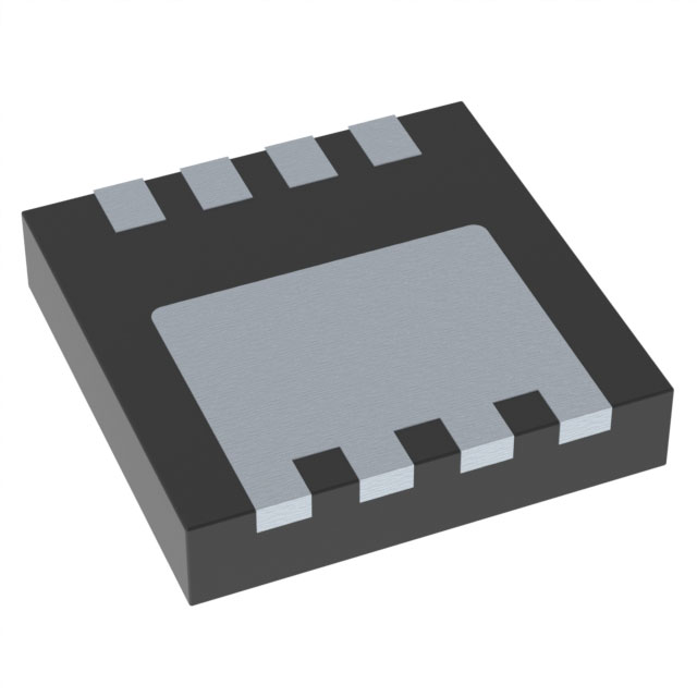
The NTTFS1D8N02P1E is a high-performance MOSFET (Metal Oxide) device designed and manufactured by onsemi, a leading semiconductor company. This N-Channel device is offered in an 8-pin PQFN package and is currently in active production, ensuring ongoing availability for new designs. With its robust technical specifications, the NTTFS1D8N02P1E is well-suited for a variety of applications in the electronics industry.
NTTFS1D8N02P1E Features
- Technology: MOSFET (Metal Oxide) - A technology known for its high input impedance and low noise characteristics.
- Drain to Source Voltage (Vdss): 25V - Capable of withstanding high voltages, making it suitable for demanding applications.
- Current - Continuous Drain (Id): 20A at 25°C (Ta) and 152A at Tc - High current capacity for efficient power management.
- Rds On (Max): 1.3mOhm @ 30A, 10V - Low on-resistance for minimal power loss.
- Gate Charge (Qg) (Max): 38 nC @ 10 V - Minimizes switching losses and improves efficiency.
- Input Capacitance (Ciss) (Max): 3159 pF @ 13 V - Low capacitance for fast switching speeds.
- Drive Voltage: 4.5V (Max Rds On), 10V (Min Rds On) - Easy to drive with a wide range of gate voltages.
- Power Dissipation: 800mW (Ta), 48W (Tc) - High power dissipation capabilities for various thermal management scenarios.
- Mounting Type: Surface Mount - Ideal for space-constrained applications and modern electronics design.
- REACH Status: REACH Unaffected - Compliant with European chemical regulations.
- RoHS Status: ROHS3 Compliant - Adheres to environmental standards restricting hazardous substances.
- Moisture Sensitivity Level (MSL): 1 (Unlimited) - Suitable for a wide range of manufacturing and storage conditions.
NTTFS1D8N02P1E Applications
The NTTFS1D8N02P1E is an ideal choice for applications requiring high efficiency, power management, and robust performance. Some specific use cases include:
- Power Electronics: In power supplies and converters where high voltage and current ratings are essential.
- Automotive Electronics: For in-vehicle power management systems that demand reliability and efficiency.
- Industrial Control Systems: In motor drives and control circuits where high power dissipation and switching speeds are crucial.
- Telecommunications: For signal processing and power management in base stations and network equipment.
Conclusion of NTTFS1D8N02P1E
The NTTFS1D8N02P1E stands out with its combination of high voltage and current ratings, low on-resistance, and fast switching capabilities. Its compliance with environmental standards and robust performance make it a preferred choice for designers looking for a reliable and efficient solution in power electronics, automotive, industrial, and telecommunications sectors. With onsemi's commitment to quality and ongoing product support, the NTTFS1D8N02P1E is a dependable component for cutting-edge electronic designs.
Tech Specifications
NTTFS1D8N02P1E Documents
Download datasheets and manufacturer documentation for NTTFS1D8N02P1E
NTTFS1D8N02P1E NTTFS1D8N02P1E onsemi RoHS onsemi REACH Related Parts


Shopping Guide


.png?x-oss-process=image/format,webp/resize,h_32)


©2025 ERSA Electronics Corporation.