
 German
 Japanese
 Portuguese
 Korea
Korea
 Mexico
 Dutch
Dutch


STMicroelectronics
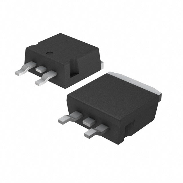
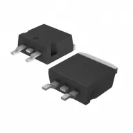
STB40NF20
Why Choose Us?
Professional Platform
B2B & B2C purchasingDelivery at full speed
1-2 days deliveryWide variety
Original manufacturers365 days guarantee
Responsible quality
.png)


Tech Specifications
STB40NF20 Description
STB40NF20 Description
The STB40NF20 is a high-performance N-Channel MOSFET from STMicroelectronics, designed for applications requiring high power and efficiency. With its advanced technology and robust features, it offers superior performance in a compact D2PAK package. This MOSFET is part of the STripFET™ series, known for its excellent trade-off between on-resistance and gate charge, resulting in high efficiency and fast switching.
STB40NF20 Features
- Technology: MOSFET (Metal Oxide), ensuring high reliability and performance.
- Drain to Source Voltage (Vdss): 200V, suitable for high-voltage applications.
- Current - Continuous Drain (Id): 40A at 25°C, providing high current handling capability.
- Rds On (Max) @ Id, Vgs: 45mOhm @ 20A, 10V, ensuring low on-resistance for high efficiency.
- Gate Charge (Qg) (Max) @ Vgs: 75 nC @ 10V, contributing to fast switching and low power consumption.
- Input Capacitance (Ciss) (Max) @ Vds: 2500 pF @ 25V, allowing for high-speed operation.
- Vgs (Max): ±20V, providing flexibility in gate voltage requirements.
- Drive Voltage (Max Rds On, Min Rds On): 10V, simplifying the design process.
- Power Dissipation (Max): 160W (Tc), suitable for high-power applications.
- Mounting Type: Surface Mount, facilitating easy integration into various designs.
- REACH Status: REACH Unaffected, ensuring compliance with environmental regulations.
- RoHS Status: ROHS3 Compliant, adhering to the latest environmental standards.
- Moisture Sensitivity Level (MSL): 1 (Unlimited), indicating high resistance to moisture-related issues.
STB40NF20 Applications
The STB40NF20 is ideal for a variety of applications where high power and efficiency are paramount. Some specific use cases include:
- Power Supplies: Due to its high voltage and current ratings, it is well-suited for power supply designs.
- Motor Controls: Its low on-resistance and high current handling make it an excellent choice for motor control applications.
- Industrial Automation: The robustness and high power dissipation capabilities make it suitable for industrial automation systems.
- Automotive Applications: The STB40NF20 can be used in various automotive applications, such as electric power steering and battery management systems, where reliability and performance are crucial.
Conclusion of STB40NF20
The STB40NF20 from STMicroelectronics stands out as a high-performance MOSFET, offering a combination of high voltage, current, and power dissipation capabilities. Its advanced features, such as low on-resistance and fast switching, make it an excellent choice for demanding applications in power supplies, motor controls, and industrial automation. With its compliance with environmental standards and robust design, the STB40NF20 is a reliable and efficient solution for high-power electronic designs.
FAQ
| Quantity | Unit Price | Ext. Price |
|---|---|---|
| 1+ | $4.22572 | $4.23 |
| 10+ | $4.12972 | $41.30 |
| 30+ | $4.06628 | $121.99 |
Not available to buy online? Want the lower wholesale price? Please Send RFQ to get best price, we will respond immediately


.png?x-oss-process=image/format,webp/resize,h_32)


