

STMicroelectronics
STF100N6F7
Single FETs, MOSFETs

Not available to buy online? Want the lower wholesale price? Please Send RFQ to get best price, we will respond immediately


.png?x-oss-process=image/format,webp/resize,p_30)


STF100N6F7 Description
STF100N6F7 Description
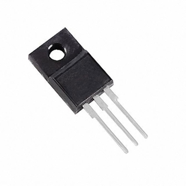
The STF100N6F7 from STMicroelectronics is a high-performance N-channel MOSFET designed for power management applications. It features a 60V drain-to-source voltage (Vdss) and a continuous drain current (Id) of 46A (Tc), making it suitable for high-current switching. Part of the STripFET™ F7 series, this MOSFET leverages advanced Metal Oxide (MOSFET) technology to deliver low on-resistance (Rds(on) of 5.6mΩ @ 23A, 10V) and high efficiency. Packaged in a TO220FP through-hole format, it ensures robust thermal performance with a maximum power dissipation of 25W (Tc).
STF100N6F7 Features
- Low Rds(on): 5.6mΩ @ 23A, 10V minimizes conduction losses, improving efficiency.
- High Current Handling: 46A continuous drain current (Tc) supports demanding power applications.
- Fast Switching: Low gate charge (Qg) of 30nC @ 10V and input capacitance (Ciss) of 1980pF @ 25V ensure rapid switching performance.
- Wide Vgs Range: ±20V gate-source voltage (Vgs) enhances flexibility in drive circuitry.
- Robust Construction: TO220FP package offers excellent thermal dissipation and mechanical durability.
- Compliance: ROHS3 compliant, REACH unaffected, and ECCN EAR99 for global regulatory adherence.
STF100N6F7 Applications
The STF100N6F7 excels in high-efficiency power conversion and switching applications, including:
- DC-DC Converters & SMPS: Low Rds(on) reduces energy loss in power supplies.
- Motor Control & Drives: High current capability supports brushed/brushless motor drivers.
- Automotive Systems: Suitable for LED drivers, battery management, and load switches in 12V/24V systems.
- Industrial Power Modules: Ideal for solar inverters, UPS, and welding equipment due to its rugged design.
Conclusion of STF100N6F7
The STF100N6F7 stands out as a high-efficiency, low-loss MOSFET with superior thermal and electrical characteristics. Its low on-resistance, high current rating, and fast switching make it a top choice for power electronics designers. Whether in automotive, industrial, or consumer applications, this MOSFET delivers reliable performance and energy savings, backed by STMicroelectronics' proven STripFET™ F7 technology.
Tech Specifications
STF100N6F7 Documents
Download datasheets and manufacturer documentation for STF100N6F7
Assembly Site 03/Oct/2023 STF100N6F7 STF100N6F7 Related Parts


Shopping Guide


.png?x-oss-process=image/format,webp/resize,h_32)


©2025 ERSA Electronics Corporation.