

STMicroelectronics
STB18NF25
Single FETs, MOSFETs

Not available to buy online? Want the lower wholesale price? Please Send RFQ to get best price, we will respond immediately


.png?x-oss-process=image/format,webp/resize,p_30)


STB18NF25 Description
STB18NF25 Description
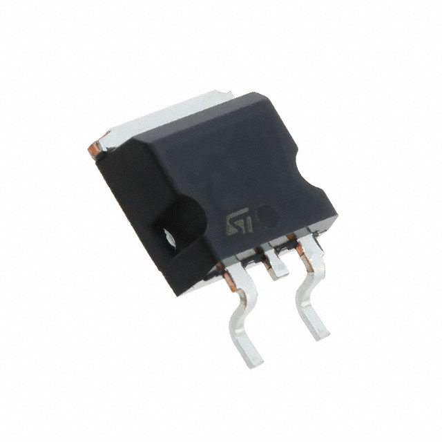
The STB18NF25 is a high-performance N-Channel MOSFET from STMicroelectronics, designed for automotive applications. This device is part of the STripFET™ II series, offering superior performance and reliability. With a drain-to-source voltage (Vdss) of 250V and a continuous drain current (Id) of 17A at 25°C, the STB18NF25 is capable of handling high-power applications. The device is available in a D2PAK package, making it suitable for surface-mount applications.
STB18NF25 Features
- Technology: MOSFET (Metal Oxide) with advanced STripFET™ II technology for improved performance.
- Input Capacitance (Ciss): Maximum 1000 pF at 25V, ensuring fast switching and reduced power consumption.
- Gate Charge (Qg): Maximum 29.5 nC at 10V, contributing to lower switching losses.
- Drain to Source Voltage (Vdss): 250V, suitable for high-voltage applications.
- Power Dissipation (Max): 110W (Tc), enabling high-power operation.
- Rds On (Max): 165mOhm at 8.5A, 10V, providing low on-resistance for efficient current flow.
- Vgs(th) (Max): 4V at 250µA, ensuring reliable gate control.
- Drive Voltage: Maximum 10V for Rds On, ensuring compatibility with various gate drivers.
- Mounting Type: Surface Mount, suitable for compact designs.
- Grade: Automotive, designed to meet the stringent requirements of automotive applications.
- RoHS Status: ROHS3 Compliant, ensuring environmental compliance.
- Moisture Sensitivity Level (MSL): 1 (Unlimited), allowing for flexible storage and handling.
STB18NF25 Applications
The STB18NF25 is ideal for a variety of high-power automotive applications, including:
- Power Management: In automotive power management systems, the STB18NF25 can efficiently handle high currents and voltages, ensuring reliable power distribution.
- Motor Control: The device's low on-resistance and high current capability make it suitable for motor control applications, such as electric power steering and electric braking systems.
- LED Lighting: In automotive LED lighting systems, the STB18NF25 can efficiently manage high currents, ensuring consistent and reliable illumination.
- Battery Management: The device can be used in battery management systems to regulate current flow and protect against overcharging and over-discharging.
Conclusion of STB18NF25
The STB18NF25 is a powerful and reliable N-Channel MOSFET from STMicroelectronics, designed for demanding automotive applications. Its advanced STripFET™ II technology, combined with its high voltage and current ratings, make it an ideal choice for power management, motor control, LED lighting, and battery management systems. With its automotive-grade design and compliance with environmental regulations, the STB18NF25 is a trusted solution for high-performance automotive electronics.
Tech Specifications
STB18NF25 Documents
Download datasheets and manufacturer documentation for STB18NF25
Mult Devices Testing 10/May/2018 ST(B,D)18NF25 Mult Dev Inner Box Chg 9/Dec/2021 Box Label Chg 28/Jul/2016 STB18NF25 View All Specifications ST(B,D)18NF25 D2PAK Lead Modification 04/Oct/2013 Related Parts


Shopping Guide


.png?x-oss-process=image/format,webp/resize,h_32)


©2025 ERSA Electronics Corporation.