
STMicroelectronics
STP140NF55
Single FETs, MOSFETs


.png?x-oss-process=image/format,webp/resize,p_30)


STP140NF55 Description
STP140NF55 Description
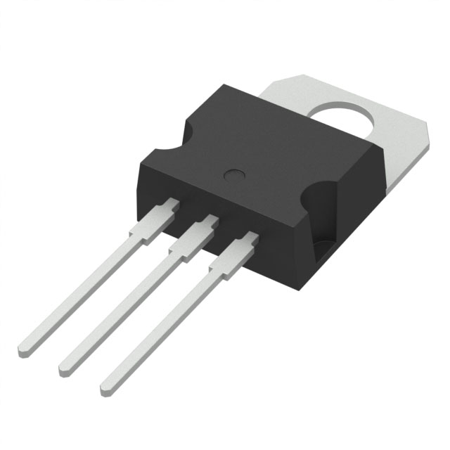
The STP140NF55 is a high-performance N-Channel MOSFET from STMicroelectronics, designed for power applications requiring high efficiency and reliability. With a drain-source voltage (Vdss) of 55V and a continuous drain current (Id) of 80A at 25°C, this device is suitable for a wide range of applications. The STP140NF55 features a low on-resistance (Rds(on)) of 8mΩ at 40A and 10V, ensuring minimal power dissipation and high efficiency. The device is mounted in a through-hole TO220AB package, making it ideal for applications requiring high power dissipation.
STP140NF55 Features
- Low On-Resistance (Rds(on)): 8mΩ at 40A and 10V, ensuring minimal power dissipation and high efficiency.
- High Drain-Source Voltage (Vdss): 55V, suitable for high-voltage applications.
- Continuous Drain Current (Id): 80A at 25°C, capable of handling high current loads.
- Low Gate Charge (Qg): 142nC at 10V, reducing switching losses and improving efficiency.
- Low Input Capacitance (Ciss): 5300pF at 25V, minimizing parasitic capacitance and improving high-frequency performance.
- Robust Gate Drive Voltage (Vgs): ±20V, providing flexibility in gate drive circuit design.
- REACH Unaffected and RoHS3 Compliant: Ensuring environmental compliance and reducing the risk of regulatory non-compliance.
STP140NF55 Applications
The STP140NF55 is ideal for various high-power applications, including:
- Power Supplies: Due to its high voltage and current ratings, the STP140NF55 is suitable for power supply applications, such as switching power supplies and battery chargers.
- Industrial Control: The device's high current and voltage ratings make it suitable for motor control and other industrial control applications.
- Automotive Applications: The STP140NF55 can be used in automotive applications, such as electric power steering and battery management systems, where high reliability and efficiency are critical.
- RF Power Amplifiers: The low on-resistance and high voltage ratings make the STP140NF55 suitable for RF power amplifiers in communication systems.
Conclusion of STP140NF55
The STP140NF55 is a high-performance N-Channel MOSFET from STMicroelectronics, offering a combination of high voltage, current, and efficiency. Its low on-resistance, low gate charge, and low input capacitance make it an ideal choice for high-power applications requiring high efficiency and reliability. With its REACH unaffected and RoHS3 compliant status, the STP140NF55 is an environmentally friendly solution for power electronics applications.
Tech Specifications
STP140NF55 Documents
Download datasheets and manufacturer documentation for STP140NF55
 STB140NF55(-1), STP140NF55
  STP140NF55 View All Specifications
  STB140NF55(-1), STP140NF55
 Shopping Guide


.png?x-oss-process=image/format,webp/resize,h_32)


