
 German
 Japanese
 Portuguese
 Korea
Korea
 Mexico
 Dutch
Dutch


STMicroelectronics
STB140NF55T4
Why Choose Us?
Professional Platform
B2B & B2C purchasingDelivery at full speed
1-2 days deliveryWide variety
Original manufacturers365 days guarantee
Responsible quality
.png)


Tech Specifications
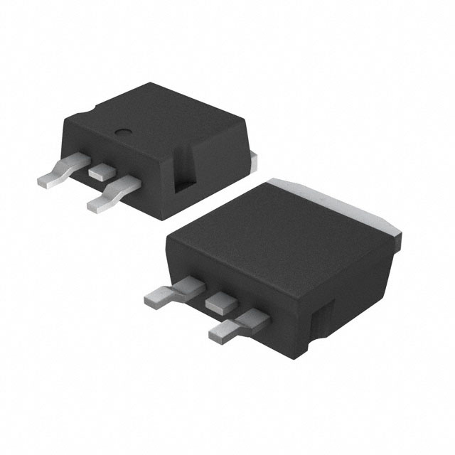
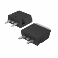
STB140NF55T4 Description
STB140NF55T4 Description
The STB140NF55T4 from STMicroelectronics is a high-performance N-channel power MOSFET designed for demanding applications requiring efficient power management. Part of the STripFET™ II series, this device offers a 55V drain-to-source voltage (Vdss) and a continuous drain current (Id) of 80A (Tc), making it suitable for high-current switching applications. Packaged in a D2PAK (TO-263) surface-mount form factor, it combines robust thermal performance with compact design. The MOSFET features a low on-resistance (Rds On) of 8mOhm at 10V gate drive, minimizing conduction losses and improving efficiency. With a gate charge (Qg) of 142nC and an input capacitance (Ciss) of 5300pF, it ensures fast switching speeds while maintaining stability.
STB140NF55T4 Features
- Low Rds On: 8mOhm @ 40A, 10V reduces power dissipation and enhances efficiency.
- High Current Handling: 80A continuous drain current (Tc) for robust performance in high-power circuits.
- Fast Switching: Optimized gate charge (142nC) and capacitance for improved switching efficiency.
- Thermal Performance: 300W power dissipation (Tc) ensures reliability under high-load conditions.
- Wide Vgs Range: ±20V gate-to-source voltage tolerance for flexible drive compatibility.
- RoHS3 & REACH Compliant: Meets environmental and safety standards for global use.
- D2PAK Package: Surface-mount design with excellent thermal conductivity for PCB integration.
STB140NF55T4 Applications
This MOSFET is ideal for:
- DC-DC Converters: Efficient power conversion in industrial and automotive systems.
- Motor Control: High-current driving in robotics, drones, and industrial automation.
- Power Supplies: Switching regulators and SMPS designs requiring low-loss operation.
- Battery Management: Protection circuits and load switches in energy storage systems.
- LED Drivers: High-efficiency lighting solutions with precise current control.
Conclusion of STB140NF55T4
The STB140NF55T4 stands out as a high-efficiency, high-current MOSFET with superior thermal and electrical characteristics. Its low Rds On, fast switching, and robust packaging make it a preferred choice for power electronics designers. Whether used in automotive, industrial, or consumer applications, this device delivers reliable performance while adhering to stringent environmental standards. For engineers seeking a balance of power handling and efficiency, the STB140NF55T4 is a compelling solution.
FAQ
| Quantity | Unit Price | Ext. Price |
|---|---|---|
| 1+ | $1.30972 | $1.31 |
| 10+ | $1.19485 | $11.95 |
| 30+ | $1.12285 | $33.69 |
| 100+ | $1.04743 | $104.74 |
| 500+ | $1.01485 | $507.43 |
Not available to buy online? Want the lower wholesale price? Please Send RFQ to get best price, we will respond immediately


.png?x-oss-process=image/format,webp/resize,h_32)


