
 German
 Japanese
 Portuguese
 Korea
Korea
 Mexico
 Dutch
Dutch


STMicroelectronics
STL115N10F7AG

Why Choose Us?
Professional Platform
B2B & B2C purchasingDelivery at full speed
1-2 days deliveryWide variety
Original manufacturers365 days guarantee
Responsible quality
.png)


Tech Specifications
STL115N10F7AG Description
STL115N10F7AG Description
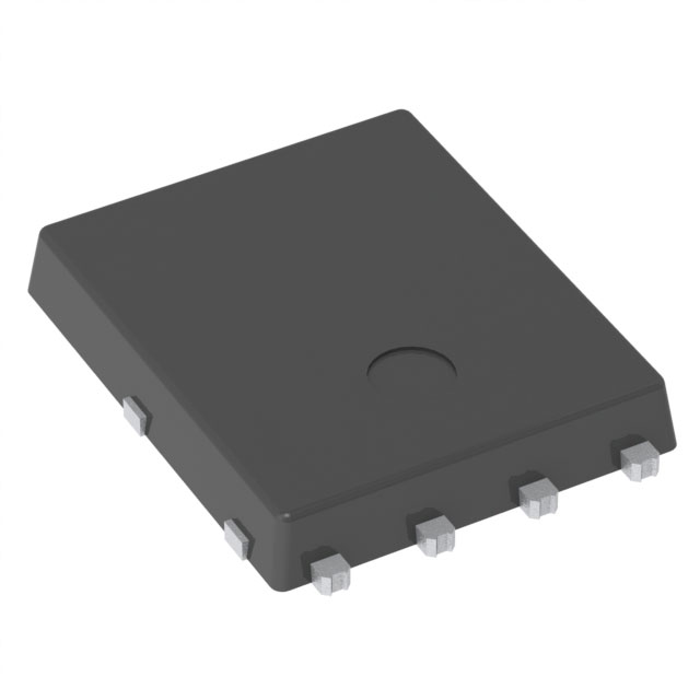
The STL115N10F7AG from STMicroelectronics is a high-performance N-channel MOSFET designed for demanding power management applications. Built using advanced STripFET™ F7 technology, it offers an optimal balance of low on-resistance (6mΩ @ 53A, 10V) and high current handling (107A continuous drain current @ 25°C). With a 100V drain-to-source voltage (Vdss) rating and a robust 136W power dissipation (Tc), this MOSFET is engineered for efficiency and reliability in high-power circuits. Its PowerFlat™ (5x6) surface-mount package with wettable flanks ensures superior thermal performance and solder joint inspection compatibility, making it ideal for automated assembly processes.
STL115N10F7AG Features
- Low Rds(On): 6mΩ @ 53A, 10V minimizes conduction losses.
- High Current Capability: 107A continuous drain current supports high-load applications.
- Fast Switching: Optimized gate charge (72.5nC @ 10V) and input capacitance (5600pF @ 50V) enhance switching efficiency.
- Automotive Grade: Compliant with stringent automotive reliability standards.
- Robust Protection: ±20V gate-source voltage (Vgs) tolerance for enhanced durability.
- Surface-Mount Design: PowerFlat™ package with wettable flanks improves thermal dissipation and manufacturability.
STL115N10F7AG Applications
This MOSFET excels in high-efficiency power systems, including:
- Automotive Systems: Motor drives, LED lighting, and DC-DC converters.
- Industrial Power Supplies: High-current switching regulators and inverters.
- Telecom Infrastructure: Base station power amplifiers and server PSUs.
- Renewable Energy: Solar inverters and battery management systems (BMS).
Its low Rds(On) and high thermal performance make it particularly suitable for space-constrained, high-reliability applications.
Conclusion of STL115N10F7AG
The STL115N10F7AG stands out as a superior choice for engineers seeking a high-efficiency, high-current MOSFET with automotive-grade reliability. Its combination of low on-resistance, fast switching, and robust packaging ensures optimal performance in demanding environments. Whether for automotive, industrial, or renewable energy applications, this device delivers the power density and thermal management required for next-generation designs.
FAQ
| Quantity | Unit Price | Ext. Price |
|---|---|---|
| 1+ | $3.36343 | $3.36 |
| 10+ | $2.88000 | $28.80 |
| 30+ | $2.59372 | $77.81 |
Not available to buy online? Want the lower wholesale price? Please Send RFQ to get best price, we will respond immediately


.png?x-oss-process=image/format,webp/resize,h_32)


