STMicroelectronics_STN4NF06L

STMicroelectronics
STN4NF06L  
Single FETs, MOSFETs

STMicroelectronics
STN4NF06L
278-STN4NF06L
Ersa
STMicroelectronics-STN4NF06L-datasheets-12986621.pdf
MOSFET N-CH 60V 4A SOT-223
In Stock : 15230

Not available to buy online? Want the lower wholesale price? Please Send RFQ to get best price, we will respond immediately

QUICK RFQ
ADD TO RFQ LIST
ersa FreeSample ersa flow
  • Quantity
  • Unit Price
  • Ext. Price
    • 1+
    • $1.06978
    • $1.07
    • 10+
    • $0.90583
    • $9.06
    • 30+
    • $0.81641
    • $24.49
    ADD TO CART
    QUICK ORDER
    $1.06978    $1.07
    ISO9001
    Quality Policy
    ISO45001
    ISO14001

    STN4NF06L Description

    STN4NF06L is a high voltage N-channel MOSFET transistor manufactured by STMicroelectronics. It is designed for use in a variety of applications, including high voltage switching and power management circuits.

    Description:

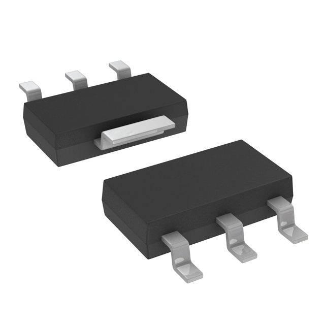
    The STN4NF06L is an N-channel enhancement mode field-effect transistor (FET). It is housed in a TO-220 package, which is a popular and widely used package for power transistors. The device has a maximum drain-source voltage (Vds) of 600V, a continuous drain current (Id) of 4.1A, and a gate-source voltage (Vgs) of ±20V.

    Features:

    • N-channel, enhancement mode
    • High voltage operation: Vds of 600V
    • High current capability: Id of 4.1A
    • Low gate charge for fast switching
    • Logic level compatible: Vgs of ±20V
    • Suitable for use in high voltage switching and power management circuits

    Applications:

    The STN4NF06L is suitable for a wide range of applications, including:

    1. Motor control and drive circuits
    2. Power management and regulation circuits
    3. High voltage switching applications
    4. Inverter circuits for renewable energy systems
    5. Battery management systems
    6. Industrial control and automation systems

    In summary, the STN4NF06L is a high voltage N-channel MOSFET transistor that offers high current capability, fast switching, and logic level compatibility. It is suitable for use in a variety of high voltage switching and power management applications.

    Tech Specifications

    Configuration
    Typical Turn-Off Delay Time (ns)
    Input Capacitance (Ciss) (Max) @ Vds
    Gate Charge (Qg) (Max) @ Vgs
    Typical Rise Time (ns)
    PPAP
    Channel Mode
    Typical Turn-On Delay Time (ns)
    Product Status
    Automotive
    Drain to Source Voltage (Vdss)
    Supplier Package
    Package / Case
    Technology
    REACH Status
    Channel Type
    EU RoHS
    Maximum Continuous Drain Current (A)
    Moisture Sensitivity Level (MSL)
    Operating Temperature
    Maximum Pulsed Drain Current @ TC=25°C (A)
    Maximum Drain Source Voltage (V)
    Maximum Drain Source Resistance (mOhm)
    ECCN
    Supplier Temperature Grade
    Mounting Type
    Rds On (Max) @ Id, Vgs
    Standard Package Name
    Vgs(th) (Max) @ Id
    Pin Count
    Mounting
    Minimum Gate Threshold Voltage (V)
    Lead Shape
    Current - Continuous Drain (Id) @ 25°C
    SVHC
    Drive Voltage (Max Rds On, Min Rds On)
    HTSUS
    Package
    Typical Gate Charge @ Vgs (nC)
    Typical Input Capacitance @ Vds (pF)
    Category
    PCB changed
    HTS
    FET Type
    Number of Elements per Chip
    ECCN (US)
    Maximum Power Dissipation (mW)
    Supplier Device Package
    Minimum Operating Temperature (°C)
    Maximum Operating Temperature (°C)
    Power Dissipation (Max)
    Typical Fall Time (ns)
    Process Technology
    Package Height
    Maximum Positive Gate Source Voltage (V)
    Mfr
    Vgs (Max)
    RoHS Status
    FET Feature
    Maximum Gate Source Voltage (V)
    SVHC Exceeds Threshold
    Package Length
    Maximum Diode Forward Voltage (V)
    Series
    Operating Junction Temperature (°C)
    Typical Output Capacitance (pF)
    Tab
    Part Status
    Maximum Gate Threshold Voltage (V)
    Package Width
    Maximum Junction Ambient Thermal Resistance on PCB (°C/W)
    Base Product Number
    Unit Weight
    Id - Continuous Drain Current
    Fall Time
    RoHS
    Qg - Gate Charge
    Tradename
    Transistor Type
    Number of Channels
    Typical Turn-On Delay Time
    Height
    Maximum Operating Temperature
    Width
    Rds On - Drain-Source Resistance
    Mounting Style
    Vgs - Gate-Source Voltage
    Typical Turn-Off Delay Time
    Transistor Polarity
    Minimum Operating Temperature
    Vds - Drain-Source Breakdown Voltage
    Qualification
    Rise Time
    Length
    Forward Transconductance - Min
    Vgs th - Gate-Source Threshold Voltage
    Pd - Power Dissipation
    USHTS

    STN4NF06L Documents

    Download datasheets and manufacturer documentation for STN4NF06L

    Ersa Mult Dev Assembly Chg 18/Oct/2019      
    Ersa STN4NF06L      
    Ersa Box Label Chg 28/Jul/2016      
    Ersa STN4NF06L View All Specifications      
    Ersa STN4NF06L      

    Shopping Guide

    Payment Methods
    Payment Methods include Prepayment TT (bank transfer), Western Union, and PayPal. Customers are responsible for shipping costs, bank charges, customs duties and taxes.
    Shipping Rate
    Shipments are made once a day around 5pm, excluding Sundays. Once shipped, the estimated delivery time is usually 5-7 business days, depending on the courier you choose.
    Delivery Methods
    Provide DHL, FedEx, UPS, EMS, SF Express and Registered Airmail International Delivery Service