

STMicroelectronics
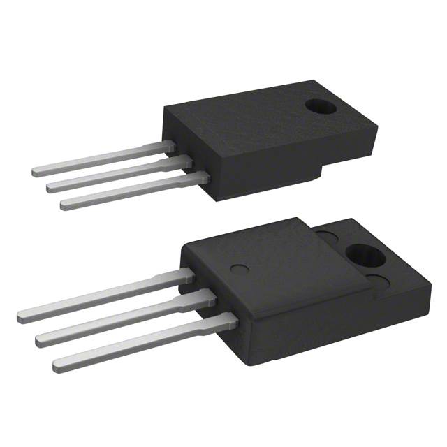
STF20N90K5
Single FETs, MOSFETs

Not available to buy online? Want the lower wholesale price? Please Send RFQ to get best price, we will respond immediately


.png?x-oss-process=image/format,webp/resize,p_30)


STF20N90K5 Description
STF20N90K5 Description
The STF20N90K5 from STMicroelectronics is a high-performance N-channel MOSFET designed for demanding power applications. Part of the MDmesh™ K5 series, it features a 900V drain-to-source voltage (Vdss) and a continuous drain current (Id) of 20A at 25°C, making it suitable for high-voltage switching. With a low on-resistance (Rds(on)) of 250mΩ at 10A, 10V, it ensures efficient power handling with minimal losses. The device is housed in a TO220FP package, offering robust thermal performance and mechanical durability. Its input capacitance (Ciss) of 1500pF @ 100V and gate charge (Qg) of 40nC @ 10V contribute to fast switching speeds, enhancing efficiency in high-frequency circuits.
STF20N90K5 Features
- High Voltage Rating: 900V Vdss for reliable operation in high-power environments.
- Low Rds(on): 250mΩ @ 10A, 10V reduces conduction losses.
- Fast Switching: Optimized gate charge (40nC) and capacitance for improved efficiency.
- Robust Thermal Performance: TO220FP package with 40W (Tc) power dissipation capability.
- Wide Gate Drive Range: Vgs(max) of ±30V for flexible drive requirements.
- Reliability: ROHS3 compliant, REACH unaffected, and MSL 1 (unlimited) for long-term stability.
- Advanced Technology: MDmesh™ K5 design ensures low switching losses and high avalanche ruggedness.
STF20N90K5 Applications
- Switched-Mode Power Supplies (SMPS): Ideal for PFC, flyback, and forward converters.
- Industrial Motor Drives: Efficient control in high-voltage motor applications.
- Renewable Energy Systems: Solar inverters and wind power converters benefit from its high voltage and low-loss characteristics.
- Lighting Solutions: Suitable for LED drivers and HID ballasts.
- Automotive Systems: Used in auxiliary power modules and EV charging systems.
Conclusion of STF20N90K5
The STF20N90K5 stands out as a high-efficiency, high-voltage MOSFET with superior performance in power electronics. Its low Rds(on), fast switching, and rugged design make it a preferred choice for industrial, automotive, and renewable energy applications. The MDmesh™ K5 technology ensures reliability under harsh conditions, while the TO220FP package provides excellent thermal management. For engineers seeking a balance of power handling, efficiency, and durability, the STF20N90K5 is a compelling solution.
Tech Specifications
STF20N90K5 Documents
Download datasheets and manufacturer documentation for STF20N90K5
STF20N90K5 STF20N90K5 Related Parts


Shopping Guide


.png?x-oss-process=image/format,webp/resize,h_32)


©2025 ERSA Electronics Corporation.