
 German
 Japanese
 Portuguese
 Korea
Korea
 Mexico
 Dutch
Dutch


STMicroelectronics
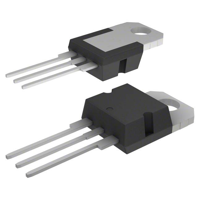
STP6N90K5

Why Choose Us?
Professional Platform
B2B & B2C purchasingDelivery at full speed
1-2 days deliveryWide variety
Original manufacturers365 days guarantee
Responsible quality
.png)


Tech Specifications
STP6N90K5 Description
STP6N90K5 Description
The STP6N90K5 is a high-performance MOSFET (Metal Oxide) from STMicroelectronics, designed for applications requiring high voltage and current capabilities. This N-Channel device is part of the MDmesh™ K5 series, offering superior performance and reliability. With a drain-to-source voltage (Vdss) of 900V and a continuous drain current (Id) of 6A at 25°C, the STP6N90K5 is ideal for demanding power electronics applications.
STP6N90K5 Features
- High Voltage and Current Ratings: The STP6N90K5 boasts a drain-to-source voltage (Vdss) of 900V and a continuous drain current (Id) of 6A at 25°C, making it suitable for high-power applications.
- Low On-Resistance: The device features a low on-resistance (Rds On) of 1.1 Ohms at a drain current of 3A and a gate-source voltage (Vgs) of 10V, ensuring efficient power dissipation.
- Robust Gate Drive Voltage: The STP6N90K5 has a maximum gate-source voltage (Vgs) of ±30V, providing flexibility in gate drive requirements.
- High Power Dissipation: With a maximum power dissipation (Pd) of 110W at the case temperature (Tc), the device can handle high power loads in various applications.
- Through-Hole Mounting: The STP6N90K5 is available in a through-hole package, providing a reliable mechanical connection for high-power applications.
- Compliance with Regulations: The device is compliant with the RoHS3 directive and is classified as REACH unaffected, ensuring environmental and regulatory compliance.
STP6N90K5 Applications
The STP6N90K5 is ideal for a wide range of high-power applications, including:
- Power Supplies: The high voltage and current ratings make it suitable for use in power supply designs, particularly in applications requiring high efficiency and reliability.
- Motor Controls: The device's robust performance characteristics make it an excellent choice for motor control applications, where high voltage and current ratings are essential.
- Industrial Automation: The STP6N90K5's high power dissipation and low on-resistance make it ideal for use in industrial automation systems, where high reliability and performance are critical.
- Renewable Energy Systems: The device's high voltage and current capabilities make it suitable for use in renewable energy systems, such as solar inverters and wind power converters.
Conclusion of STP6N90K5
The STP6N90K5 from STMicroelectronics is a high-performance MOSFET designed for demanding power electronics applications. Its high voltage and current ratings, low on-resistance, and robust gate drive voltage make it an ideal choice for power supplies, motor controls, industrial automation, and renewable energy systems. With its compliance with environmental and regulatory standards, the STP6N90K5 offers a reliable and efficient solution for high-power applications.
FAQ
Not available to buy online? Want the lower wholesale price? Please Send RFQ to get best price, we will respond immediately


.png?x-oss-process=image/format,webp/resize,h_32)


