
STMicroelectronics
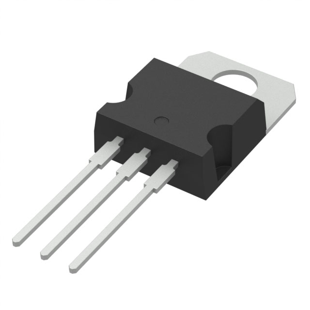
STP110N8F6
Single FETs, MOSFETs


- 1+
- $0.80813
- $0.81
- 10+
- $0.69386
- $6.94
- 50+
- $0.55973
- $27.99
- 100+
- $0.49349
- $49.35
- 500+
- $0.47196
- $235.98
- 1000+
- $0.45871
- $458.71

.png?x-oss-process=image/format,webp/resize,p_30)


STP110N8F6 Description
The STP110N8F6 is a high-power MOSFET (Metal-Oxide-Semiconductor Field-Effect Transistor) manufactured by STMicroelectronics. Here's a brief description, features, and applications of the STP110N8F6:
Description:
The STP110N8F6 is a N-channel power MOSFET with a drain-source voltage (VDS) of 60V and a continuous drain current (ID) of 110A. It is designed for use in a wide range of power electronic applications where high efficiency, fast switching, and low on-state resistance are required.
Features:
- High Power Rating: With a drain-source voltage (VDS) of 60V and a continuous drain current (ID) of 110A, the STP110N8F6 is suitable for high-power applications.
- Low On-State Resistance (RDS(on)): The MOSFET has a low on-state resistance, which minimizes power dissipation and improves efficiency in power conversion applications.
- Fast Switching Speed: The device offers fast switching capabilities, making it suitable for applications that require rapid transient response.
- Integrated Protection Features: The STP110N8F6 includes built-in protection features such as over-voltage, over-current, and over-temperature protection to ensure reliable operation and longevity.
- High-Temperature Operation: The MOSFET is designed for operation in high-temperature environments, with a maximum junction temperature (Tj) of 175°C.
- Robustness: The device is built to withstand high-energy transients and electrostatic discharge (ESD) events, making it suitable for use in harsh environments.
Applications:
- Motor Control: The STP110N8F6 can be used in motor control applications, such as electric vehicles, industrial automation, and robotics, where high power and fast switching are required.
- Power Supplies: The MOSFET is suitable for use in power supply applications, including switched-mode power supplies (SMPS) and uninterruptible power supplies (UPS), due to its high efficiency and fast switching capabilities.
- Solar Energy Systems: The STP110N8F6 can be used in solar energy systems for power conversion and management, taking advantage of its high power rating and robustness.
- Battery Management Systems: The MOSFET can be employed in battery management systems for electric vehicles and energy storage systems, where high current handling and fast switching are essential.
- Industrial Control Systems: The device can be used in various industrial control systems, such as variable frequency drives (VFDs) and servo drives, where high power and efficient power conversion are required.
Please note that this information is based on the general specifications and features of the STP110N8F6. For detailed technical specifications, electrical characteristics, and application guidelines, it is essential to refer to the official datasheet provided by STMicroelectronics.
Tech Specifications
STP110N8F6 Documents
Download datasheets and manufacturer documentation for STP110N8F6
 STP110N8F6
  EOL 09/Nov/2023
  STP110N8F6
 Shopping Guide


.png?x-oss-process=image/format,webp/resize,h_32)


