
 German
 Japanese
 Portuguese
 Korea
Korea
 Mexico
 Dutch
Dutch


STMicroelectronics
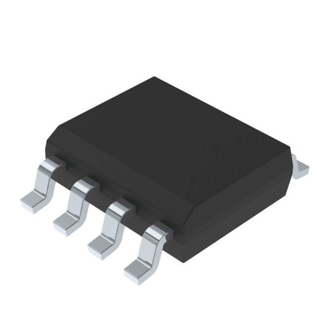
STS8N6LF6AG

Why Choose Us?
Professional Platform
B2B & B2C purchasingDelivery at full speed
1-2 days deliveryWide variety
Original manufacturers365 days guarantee
Responsible quality
.png)


Tech Specifications
STS8N6LF6AG Description
STS8N6LF6AG Description
The STS8N6LF6AG is a high-performance N-Channel MOSFET from STMicroelectronics, designed for automotive applications. It offers a robust 60V drain-to-source voltage and can handle a continuous drain current of 8A at 25°C. With a maximum power dissipation of 3.2W, this MOSFET is well-suited for demanding applications.
STS8N6LF6AG Features
- Technology: MOSFET (Metal Oxide), leveraging advanced technology for reliable performance.
- Grade: Automotive, ensuring durability and reliability in harsh environments.
- Mounting Type: Surface Mount, facilitating easy integration into circuit boards.
- Rds On (Max) @ Id, Vgs: 24mOhm @ 4A, 10V, providing low on-resistance for efficient power management.
- Vgs(th) (Max) @ Id: 2.5V @ 250µA, ensuring consistent threshold voltage for reliable operation.
- Series: STripFET™ F6, known for its excellent performance and efficiency.
- Input Capacitance (Ciss) (Max) @ Vds: 1340 pF @ 25 V, minimizing capacitance for faster switching.
- Gate Charge (Qg) (Max) @ Vgs: 27 nC @ 10 V, reducing switching losses and improving efficiency.
STS8N6LF6AG Applications
The STS8N6LF6AG is ideal for a variety of automotive applications where high voltage and current handling are required. Some specific use cases include:
- Power Management Systems: Efficiently managing power in automotive electronics.
- Motor Control: Driving electric motors in electric vehicles and other automotive systems.
- Battery Protection Circuits: Safeguarding batteries from overcurrent and overvoltage conditions.
Conclusion of STS8N6LF6AG
The STS8N6LF6AG stands out due to its automotive-grade performance, low on-resistance, and robust voltage and current ratings. Its advanced features make it a preferred choice for demanding automotive applications where reliability and efficiency are paramount. With its unique combination of performance and durability, the STS8N6LF6AG is a valuable component in the design of modern automotive systems.
FAQ
| Quantity | Unit Price | Ext. Price |
|---|---|---|
| 10+ | $0.69464 | $6.95 |
| 30+ | $0.62111 | $18.63 |
| 100+ | $0.54488 | $54.49 |
| 500+ | $0.51079 | $255.39 |
| 1000+ | $0.49608 | $496.08 |
Not available to buy online? Want the lower wholesale price? Please Send RFQ to get best price, we will respond immediately


.png?x-oss-process=image/format,webp/resize,h_32)


