
 German
 Japanese
 Portuguese
 Korea
Korea
 Mexico
 Dutch
Dutch


STMicroelectronics
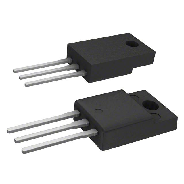
STF12N65M5

Why Choose Us?
Professional Platform
B2B & B2C purchasingDelivery at full speed
1-2 days deliveryWide variety
Original manufacturers365 days guarantee
Responsible quality
.png)


Tech Specifications
STF12N65M5 Description
STF12N65M5 Description
The STF12N65M5 is a high-performance MOSFET (Metal Oxide) from STMicroelectronics, designed for applications requiring high voltage and current handling capabilities. With a drain-to-source voltage (Vdss) of 650V and a continuous drain current (Id) of 8.5A at 25°C, this N-channel device is well-suited for various power electronics applications.
STF12N65M5 Features
- High Voltage and Current Ratings: The STF12N65M5 boasts a drain-to-source voltage of 650V and a continuous drain current of 8.5A at 25°C, making it ideal for high-power applications.
- Low On-Resistance: With a maximum Rds(on) of 430mOhm at 4.3A and 10V, this device offers low conduction losses, improving overall efficiency.
- Robust Gate Drive: The STF12N65M5 features a maximum gate-source voltage (Vgs) of ±25V, ensuring reliable operation across a wide range of gate drive conditions.
- Low Gate Charge: A maximum gate charge (Qg) of 22nC at 10V contributes to faster switching speeds and reduced switching losses.
- Thermal Management: The device can dissipate up to 25W of power, making it suitable for applications with high thermal demands.
- Environmental Compliance: The STF12N65M5 is REACH unaffected and RoHS3 compliant, ensuring compliance with environmental regulations.
STF12N65M5 Applications
The STF12N65M5 is ideal for a variety of power electronics applications, including:
- Power Supplies: Due to its high voltage and current ratings, this MOSFET is well-suited for use in power supply designs, particularly in switch-mode power supplies (SMPS) and power factor correction (PFC) circuits.
- Motor Control: The STF12N65M5's low on-resistance and high current capabilities make it an excellent choice for motor control applications, such as electric vehicle (EV) motor drives and industrial motor control systems.
- Industrial Automation: This MOSFET's robust performance characteristics make it suitable for use in industrial automation equipment, including robotics and automated machinery.
Conclusion of STF12N65M5
The STF12N65M5 from STMicroelectronics is a versatile and high-performance MOSFET, offering a combination of high voltage and current ratings, low on-resistance, and robust gate drive capabilities. Its compliance with environmental regulations and suitability for a wide range of power electronics applications make it an excellent choice for designers looking to optimize performance and efficiency in their next-generation products.
FAQ
Not available to buy online? Want the lower wholesale price? Please Send RFQ to get best price, we will respond immediately


.png?x-oss-process=image/format,webp/resize,h_32)


