
STMicroelectronics
STW18N65M5
Single FETs, MOSFETs


.png?x-oss-process=image/format,webp/resize,p_30)


STW18N65M5 Description
STW18N65M5 Description
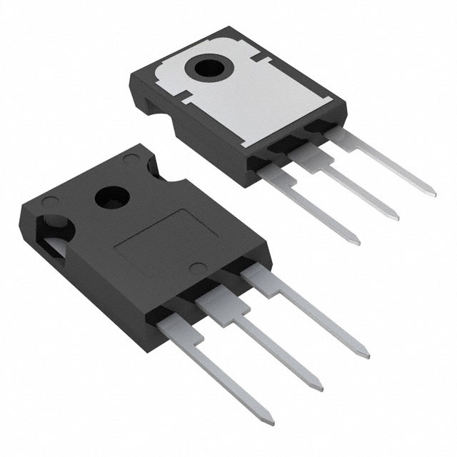
The STW18N65M5 from STMicroelectronics is a high-performance N-channel MOSFET designed for demanding power applications. Built using advanced MDmesh™ V technology, it offers a robust 650V drain-to-source voltage (Vdss) rating and a continuous drain current (Id) of 15A (Tc). With an Rds(on) as low as 220mΩ at 10V gate drive, this device ensures efficient power handling while minimizing conduction losses. The MOSFET operates reliably up to 150°C junction temperature (TJ), making it suitable for high-temperature environments. Packaged in a TO-247 through-hole format, it provides excellent thermal dissipation, supporting a maximum power dissipation of 110W (Tc).
STW18N65M5 Features
- High Voltage & Current Rating: 650V Vdss and 15A Id ensure robust performance in high-power circuits.
- Low Rds(on): 220mΩ @ 10V reduces conduction losses, improving efficiency.
- MDmesh™ V Technology: Enhances switching performance and reduces gate charge (Qg: 31nC @ 10V).
- Wide Gate-Source Voltage Range: Supports ±25V Vgs, offering flexibility in drive circuitry.
- Thermal Efficiency: TO-247 package with high power dissipation (110W) for effective heat management.
- Reliability: RoHS3 compliant, REACH unaffected, and MSL 1 (unlimited) for long-term durability.
STW18N65M5 Applications
The STW18N65M5 is ideal for:
- Switched-Mode Power Supplies (SMPS): High efficiency and low losses make it perfect for AC-DC converters.
- Motor Drives & Inverters: Robust voltage handling suits industrial motor control systems.
- Solar Inverters & Energy Storage: High-temperature tolerance ensures reliability in renewable energy applications.
- Induction Heating & Welding Equipment: Fast switching and low Rds(on) enhance performance in high-frequency circuits.
Conclusion of STW18N65M5
The STW18N65M5 stands out as a high-efficiency, high-reliability MOSFET for power electronics. Its low Rds(on), high voltage capability, and advanced MDmesh™ V technology make it superior to conventional MOSFETs in efficiency-critical applications. Whether in industrial motor drives, renewable energy systems, or high-power SMPS, this device delivers optimal performance, thermal stability, and long-term durability, making it a top choice for engineers designing next-generation power solutions.
Tech Specifications
STW18N65M5 Documents
Download datasheets and manufacturer documentation for STW18N65M5
 STx18N65M5
  Standard outer labelling 15/Nov/2023
  STW18N65M5 View All Specifications
  STx18N65M5
 Shopping Guide


.png?x-oss-process=image/format,webp/resize,h_32)


