
STMicroelectronics
STB30N65M5
Single FETs, MOSFETs

Not available to buy online? Want the lower wholesale price? Please Send RFQ to get best price, we will respond immediately


.png?x-oss-process=image/format,webp/resize,p_30)


STB30N65M5 Description
STB30N65M5 Description
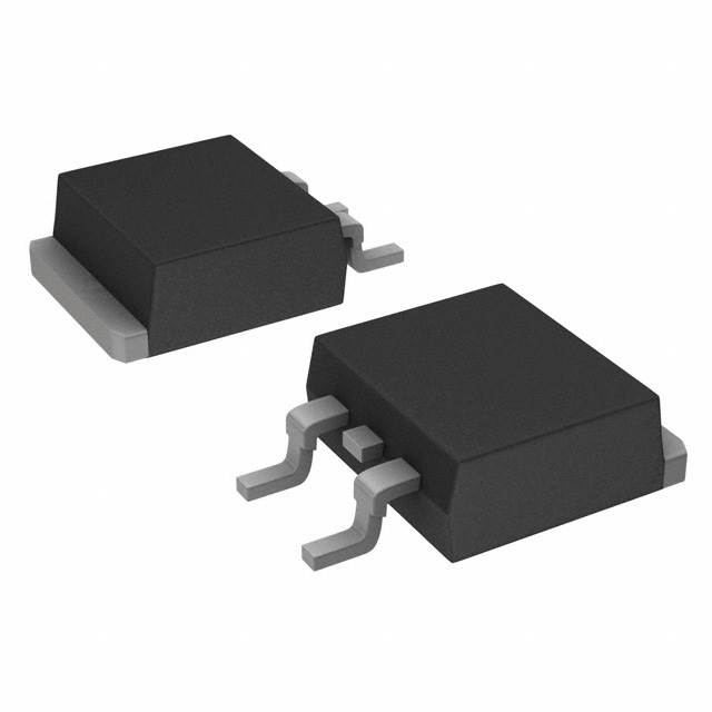
The STB30N65M5 is a high-performance MOSFET N-CH 650V 22A D2PAK from STMicroelectronics. It is designed for applications requiring high power and efficiency. With its advanced technology and robust design, the STB30N65M5 offers excellent electrical characteristics and reliability. It is manufactured using STMicroelectronics' proprietary MDmesh™ V technology, ensuring superior performance and longevity.
STB30N65M5 Features
- Technology: MOSFET (Metal Oxide) using STMicroelectronics' MDmesh™ V technology
- Drain to Source Voltage (Vdss): 650V
- Current - Continuous Drain (Id) @ 25°C: 22A (Tc)
- Rds On (Max) @ Id, Vgs: 139mOhm @ 11A, 10V
- Gate Charge (Qg) (Max) @ Vgs: 64 nC @ 10 V
- Input Capacitance (Ciss) (Max) @ Vds: 2880 pF @ 100 V
- Vgs (Max): ±25V
- Vgs(th) (Max) @ Id: 5V @ 250µA
- Drive Voltage (Max Rds On, Min Rds On): 10V
- Power Dissipation (Max): 140W (Tc)
- Operating Temperature: 150°C (TJ)
- Mounting Type: Surface Mount
- Moisture Sensitivity Level (MSL): 1 (Unlimited)
- REACH Status: REACH Unaffected
- RoHS Status: ROHS3 Compliant
- Package: D2PAK, Tape & Reel (TR)
STB30N65M5 Applications
The STB30N65M5 is ideal for a wide range of applications due to its high power rating and excellent electrical characteristics. Some specific use cases include:
- Industrial Motor Control: The high voltage and current ratings make it suitable for motor control applications in industrial settings.
- Power Supplies: The STB30N65M5 can be used in power supply designs requiring high efficiency and reliability.
- Automotive Applications: Its robust design and high temperature rating make it suitable for automotive applications, such as electric vehicle charging systems.
- Renewable Energy Systems: The STB30N65M5 can be used in solar inverters and wind turbine power electronics.
Conclusion of STB30N65M5
The STB30N65M5 from STMicroelectronics is a powerful and reliable MOSFET designed for high-power applications. Its advanced MDmesh™ V technology, high voltage and current ratings, and excellent electrical characteristics make it an ideal choice for a wide range of applications, including industrial motor control, power supplies, automotive systems, and renewable energy. The STB30N65M5's unique features and advantages over similar models, such as its low Rds On and high power dissipation, make it a preferred choice for demanding applications where performance and reliability are critical.
Tech Specifications
STB30N65M5 Documents
Download datasheets and manufacturer documentation for STB30N65M5
STx30N65M5 Mult Dev Inner Box Chg 9/Dec/2021 STB30N65M5 View All Specifications STx30N65M5 IPG-PWR/14/8422 11/Apr/2014 D2PAK Lead Modification 04/Oct/2013 Related Parts


Shopping Guide


.png?x-oss-process=image/format,webp/resize,h_32)


©2025 ERSA Electronics Corporation.