
 German
 Japanese
 Portuguese
 Korea
Korea
 Mexico
 Dutch
Dutch


STMicroelectronics
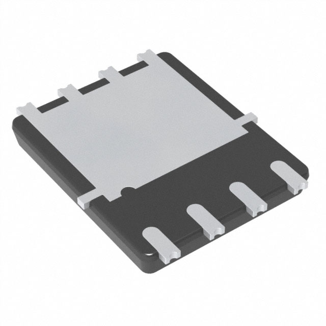
STLD200N4F6AG

Why Choose Us?
Professional Platform
B2B & B2C purchasingDelivery at full speed
1-2 days deliveryWide variety
Original manufacturers365 days guarantee
Responsible quality
.png)


Tech Specifications
STLD200N4F6AG Description
STLD200N4F6AG is a low-side MOSFET driver from STMicroelectronics. It is designed to drive N-channel MOSFETs in a wide range of applications, including motor control, power management, and automotive systems.
Description:
The STLD200N4F6AG is a monolithic integrated circuit in a compact DFN6 package. It features a high-voltage input with a logic-level output, allowing it to interface with low-voltage microcontrollers and drive high-voltage MOSFETs. The device also includes built-in protection features such as overcurrent protection, undervoltage lockout, and short-circuit protection.
Features:
- Low input voltage: The STLD200N4F6AG can be driven by low-voltage microcontrollers, making it suitable for battery-powered applications.
- High output voltage: The device can drive N-channel MOSFETs with voltage ratings up to 60V, making it suitable for a wide range of power management applications.
- Overcurrent protection: The STLD200N4F6AG includes overcurrent protection to prevent damage to the MOSFETs in the event of a short circuit or overload.
- Undervoltage lockout: The device includes an undervoltage lockout feature to prevent it from operating if the input voltage falls below a certain threshold.
- Short-circuit protection: The STLD200N4F6AG includes short-circuit protection to protect the MOSFETs from damage in the event of a short circuit.
Applications:
The STLD200N4F6AG is suitable for a wide range of applications, including:
- Motor control: The device can be used to drive the MOSFETs in brushless DC motor controllers, stepper motor drivers, and other motor control applications.
- Power management: The STLD200N4F6AG can be used to drive MOSFETs in power management applications such as battery chargers, power supplies, and energy harvesting systems.
- Automotive systems: The device is suitable for use in automotive systems such as electric power steering, fuel pumps, and air conditioning systems.
- Industrial control: The STLD200N4F6AG can be used to drive MOSFETs in industrial control applications such as conveyor systems, robotic arms, and manufacturing equipment.
Overall, the STLD200N4F6AG is a versatile MOSFET driver that offers a range of features and protections to ensure reliable operation in a variety of applications. Its compact size and low input voltage make it well-suited for space-constrained and battery-powered systems.
FAQ
Not available to buy online? Want the lower wholesale price? Please Send RFQ to get best price, we will respond immediately


.png?x-oss-process=image/format,webp/resize,h_32)


