
 German
 Japanese
 Portuguese
 Korea
Korea
 Mexico
 Dutch
Dutch


STMicroelectronics
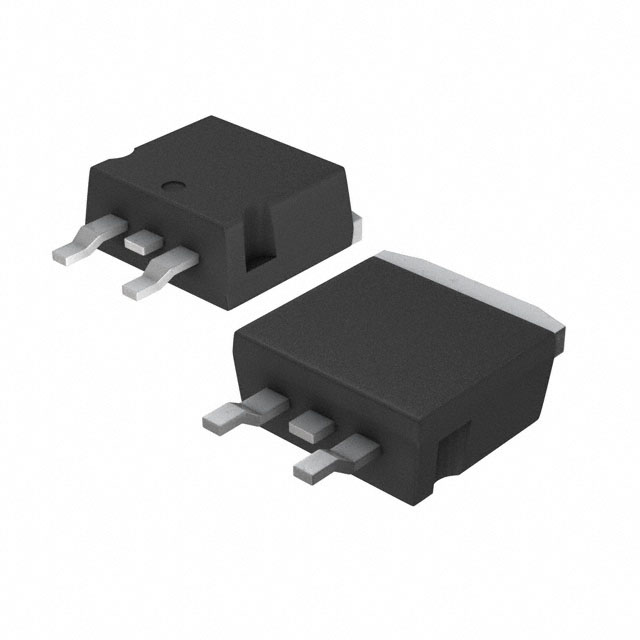
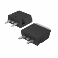
STB20NM50T4
Why Choose Us?
Professional Platform
B2B & B2C purchasingDelivery at full speed
1-2 days deliveryWide variety
Original manufacturers365 days guarantee
Responsible quality
.png)


Tech Specifications
STB20NM50T4 Description
STB20NM50T4 Description
The STB20NM50T4 is a high-performance N-Channel MOSFET from STMicroelectronics, designed for applications requiring high voltage and current handling capabilities. It features a D2PAK package and is part of the MDmesh™ series, offering superior thermal performance and reliability. With a drain-to-source voltage (Vdss) of 550V and a continuous drain current (Id) of 20A at 25°C, the STB20NM50T4 is ideal for demanding power electronic applications.
STB20NM50T4 Features
- High Voltage and Current Handling: The STB20NM50T4 can handle a maximum drain-to-source voltage of 550V and a continuous drain current of 20A at 25°C, making it suitable for high-power applications.
- Low On-Resistance: With a maximum Rds(on) of 250mOhm at 10A and 10V, the STB20NM50T4 offers low conduction losses, improving efficiency in power conversion systems.
- Fast Switching Speed: The device has a low gate charge (Qg) of 56nC at 10V and a threshold voltage (Vgs(th)) of 5V at 250µA, enabling fast switching and reducing switching losses.
- Robust Thermal Performance: The D2PAK package provides excellent thermal dissipation, ensuring reliable operation in high-power applications.
- Compliance and Environmental: The STB20NM50T4 is REACH unaffected and RoHS3 compliant, making it suitable for environmentally conscious designs.
STB20NM50T4 Applications
The STB20NM50T4 is ideal for a wide range of power electronic applications, including:
- Power Supplies: Its high voltage and current ratings make it suitable for power supply designs, such as SMPS (Switched-Mode Power Supplies) and DC-DC converters.
- Motor Drives: The device's low on-resistance and fast switching capabilities are beneficial in motor drive applications, improving efficiency and reducing losses.
- Industrial Control: The STB20NM50T4 can be used in industrial control systems, such as motor control and power distribution, where high voltage and current handling are required.
- Automotive Applications: The device's robustness and compliance with environmental regulations make it suitable for automotive applications, such as electric vehicle charging systems and power management.
Conclusion of STB20NM50T4
The STB20NM50T4 is a versatile and high-performance N-Channel MOSFET from STMicroelectronics, offering a combination of high voltage and current handling capabilities, low on-resistance, and fast switching speeds. Its robust thermal performance and compliance with environmental regulations make it an ideal choice for a wide range of power electronic applications, including power supplies, motor drives, industrial control, and automotive systems. With its unique features and advantages over similar models, the STB20NM50T4 is a reliable and efficient solution for demanding power electronic designs.
FAQ
| Quantity | Unit Price | Ext. Price |
|---|---|---|
| 1+ | $7.42457 | $7.42 |
| 10+ | $7.26172 | $72.62 |
| 30+ | $7.15372 | $214.61 |
Not available to buy online? Want the lower wholesale price? Please Send RFQ to get best price, we will respond immediately


.png?x-oss-process=image/format,webp/resize,h_32)


