
 German
 Japanese
 Portuguese
 Korea
Korea
 Mexico
 Dutch
Dutch


STMicroelectronics
STP17NF25

Why Choose Us?
Professional Platform
B2B & B2C purchasingDelivery at full speed
1-2 days deliveryWide variety
Original manufacturers365 days guarantee
Responsible quality
.png)


Tech Specifications
STP17NF25 Description
STP17NF25 Description
The STP17NF25 is a high-performance N-Channel MOSFET from STMicroelectronics, designed to deliver exceptional performance in various electronic applications. With a drain-to-source voltage (Vdss) of 250V and a continuous drain current (Id) of 17A at 25°C, this MOSFET is well-suited for high-power applications. The device features a low on-resistance (Rds On) of 165mOhm at 8.5A and 10V, ensuring efficient power dissipation and minimal power loss. The STP17NF25 is manufactured using advanced MOSFET technology, ensuring high reliability and performance.
STP17NF25 Features
- Low On-Resistance (Rds On): 165mOhm at 8.5A and 10V, ensuring efficient power dissipation and minimal power loss.
- High Drain-to-Source Voltage (Vdss): 250V, suitable for high-power applications.
- Continuous Drain Current (Id): 17A at 25°C, providing high current handling capability.
- Low Gate Threshold Voltage (Vgs(th)): 4V at 250µA, ensuring easy gate drive and low power consumption.
- Low Gate Charge (Qg): 29.5 nC at 10V, reducing switching losses and improving efficiency.
- Robust Input Capacitance (Ciss): 1000 pF at 25V, providing fast response times and high-frequency operation.
- Compliance with Industry Standards: RoHS3 compliant, REACH unaffected, and moisture sensitivity level (MSL) 1, ensuring environmental and safety compliance.
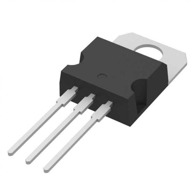
- Package Type: Through-hole TO220AB, providing easy integration and mounting in various applications.
STP17NF25 Applications
The STP17NF25 is ideal for a wide range of applications where high power, efficiency, and reliability are critical. Some specific use cases include:
- Power Supplies: Due to its high voltage and current ratings, the STP17NF25 is well-suited for power supply applications, such as switching power supplies and battery chargers.
- Motor Control: The device's high current handling capability and low on-resistance make it ideal for motor control applications, including brushless DC motors and stepper motors.
- Industrial Automation: The STP17NF25's robust performance and compliance with industry standards make it suitable for industrial automation applications, such as robotics and control systems.
- Automotive Applications: The device's high voltage and current ratings, along with its low on-resistance, make it suitable for automotive applications, such as electric vehicle charging and power management systems.
Conclusion of STP17NF25
The STP17NF25 is a high-performance N-Channel MOSFET from STMicroelectronics, offering a combination of high voltage, current, and low on-resistance, making it ideal for a wide range of high-power applications. Its robust performance, compliance with industry standards, and ease of integration make it a preferred choice for power supplies, motor control, industrial automation, and automotive applications. With its advanced MOSFET technology and STMicroelectronics' reputation for quality, the STP17NF25 is a reliable and efficient solution for demanding electronic applications.
FAQ
| Quantity | Unit Price | Ext. Price |
|---|---|---|
| 1+ | $1.77772 | $1.78 |
| 10+ | $1.48628 | $14.86 |
| 50+ | $1.32685 | $66.34 |
Not available to buy online? Want the lower wholesale price? Please Send RFQ to get best price, we will respond immediately


.png?x-oss-process=image/format,webp/resize,h_32)


