
STMicroelectronics
STW69N65M5
Single FETs, MOSFETs


.png?x-oss-process=image/format,webp/resize,p_30)


STW69N65M5 Description
STW69N65M5 Description
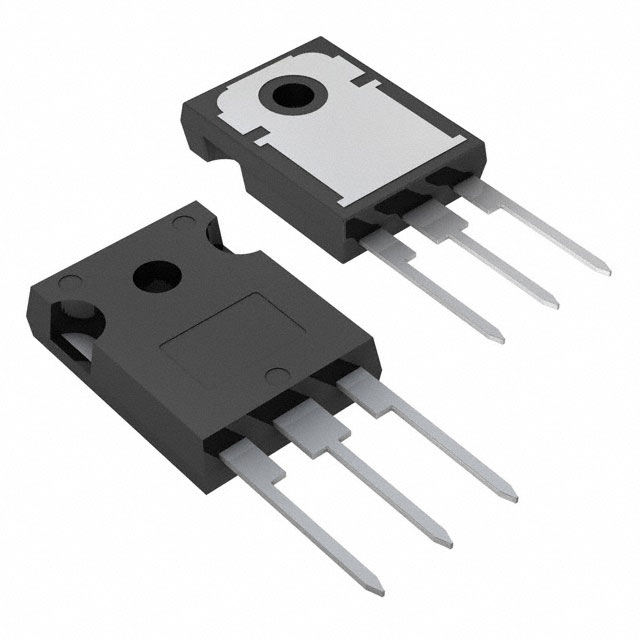
The STW69N65M5 is a high-performance N-channel MOSFET designed and manufactured by STMicroelectronics. This device is part of the MDmesh™ V series and is offered in a TO247 package. With its robust technical specifications, the STW69N65M5 is an ideal choice for demanding applications that require high power dissipation and efficient performance.
STW69N65M5 Features
- Technology: MOSFET (Metal Oxide) - Ensures high efficiency and low power loss.
- Drain to Source Voltage (Vdss): 650V - Capable of withstanding high voltages in various applications.
- Current - Continuous Drain (Id) @ 25°C: 58A (Tc) - Delivers substantial current for high-power applications.
- Rds On (Max) @ Id, Vgs: 45mOhm @ 29A, 10V - Offers low on-resistance for efficient power management.
- Gate Charge (Qg) (Max) @ Vgs: 143 nC @ 10 V - Minimizes switching losses and improves efficiency.
- Input Capacitance (Ciss) (Max) @ Vds: 6420 pF @ 100 V - Facilitates faster switching speeds.
- Operating Temperature: 150°C (TJ) - Suitable for high-temperature environments.
- Mounting Type: Through Hole - Provides a secure and reliable connection in various circuit designs.
- Power Dissipation (Max): 330W (Tc) - Capable of handling high power dissipation in demanding applications.
STW69N65M5 Applications
The STW69N65M5 is ideal for a variety of applications where high power, efficiency, and reliability are paramount. Some specific use cases include:
- Industrial Automation: Due to its high power dissipation and robust design, the STW69N65M5 is well-suited for motor control and power conversion in industrial settings.
- Automotive Electronics: The device's ability to handle high voltages and currents makes it an excellent choice for automotive applications, such as electric vehicle charging systems and power management.
- Power Supplies: The STW69N65M5's low on-resistance and high current capabilities make it ideal for use in power supply designs, where efficiency and reliability are critical.
Conclusion of STW69N65M5
The STW69N65M5 from STMicroelectronics is a high-performance N-channel MOSFET that offers a combination of high power dissipation, low on-resistance, and robust design. Its unique features and advantages make it an ideal choice for a wide range of applications, including industrial automation, automotive electronics, and power supplies. With its technical specifications and performance benefits, the STW69N65M5 stands out as a reliable and efficient solution in the electronics industry.
Tech Specifications
STW69N65M5 Documents
Download datasheets and manufacturer documentation for STW69N65M5
 IPG-PWR/14/8674 02/Sep/2014
  ST(F)W69N65M5
  Standard outer labelling 15/Nov/2023
  STW69N65M5 View All Specifications
  ST(F)W69N65M5
 Shopping Guide


.png?x-oss-process=image/format,webp/resize,h_32)


