
 German
 Japanese
 Portuguese
 Korea
Korea
 Mexico
 Dutch
Dutch


STMicroelectronics
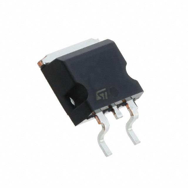
STB18N65M5

Why Choose Us?
Professional Platform
B2B & B2C purchasingDelivery at full speed
1-2 days deliveryWide variety
Original manufacturers365 days guarantee
Responsible quality
.png)


Tech Specifications
STB18N65M5 Description
STB18N65M5 Description
The STB18N65M5 from STMicroelectronics is a high-performance N-channel MOSFET designed for demanding power applications. Built using MDmesh™ V technology, it offers an optimal balance of low on-resistance (220mΩ @ 10V, 7.5A) and high breakdown voltage (650V), making it ideal for high-efficiency switching circuits. With a continuous drain current (Id) of 15A (Tc) and a power dissipation capability of 110W (Tc), this device excels in high-power environments. Its low gate charge (31nC @ 10V) and input capacitance (1240pF @ 100V) ensure fast switching speeds, reducing switching losses in high-frequency applications. The MOSFET is housed in a D2PAK (TO-263) surface-mount package, suitable for automated assembly processes.
STB18N65M5 Features
- High Voltage & Current Handling: 650V Vdss and 15A Id for robust performance in power circuits.
- Low Rds(on): 220mΩ @ 10V, 7.5A minimizes conduction losses, improving efficiency.
- Fast Switching: Low Qg (31nC) and Ciss (1240pF) enable high-frequency operation.
- Thermal Performance: 150°C max junction temperature (TJ) and 110W power dissipation ensure reliability under thermal stress.
- Wide Gate Drive Range: ±25V Vgs(max) offers flexibility in drive circuit design.
- Advanced Technology: MDmesh™ V provides superior switching performance and reduced EMI.
- Compliance: ROHS3, REACH Unaffected, ECCN EAR99, and MSL1 (Unlimited) for global compatibility.
STB18N65M5 Applications
- Switched-Mode Power Supplies (SMPS): High-voltage DC-DC converters, PFC stages.
- Motor Drives & Inverters: Efficient switching in industrial and automotive motor control.
- Renewable Energy Systems: Solar inverters, wind power converters.
- Industrial Power Systems: UPS, welding equipment, and high-power LED drivers.
- Consumer Electronics: High-efficiency adapters and power supplies.
Conclusion of STB18N65M5
The STB18N65M5 stands out as a high-reliability 650V MOSFET with low Rds(on), fast switching, and excellent thermal performance, making it a top choice for power electronics designers. Its MDmesh™ V technology ensures superior efficiency in high-frequency applications, while its D2PAK package supports automated manufacturing. Ideal for SMPS, motor drives, and renewable energy systems, this MOSFET combines performance, durability, and compliance with global standards, offering a competitive edge in demanding power applications.
FAQ
Not available to buy online? Want the lower wholesale price? Please Send RFQ to get best price, we will respond immediately


.png?x-oss-process=image/format,webp/resize,h_32)


