
 German
 Japanese
 Portuguese
 Korea
Korea
 Mexico
 Dutch
Dutch


STMicroelectronics
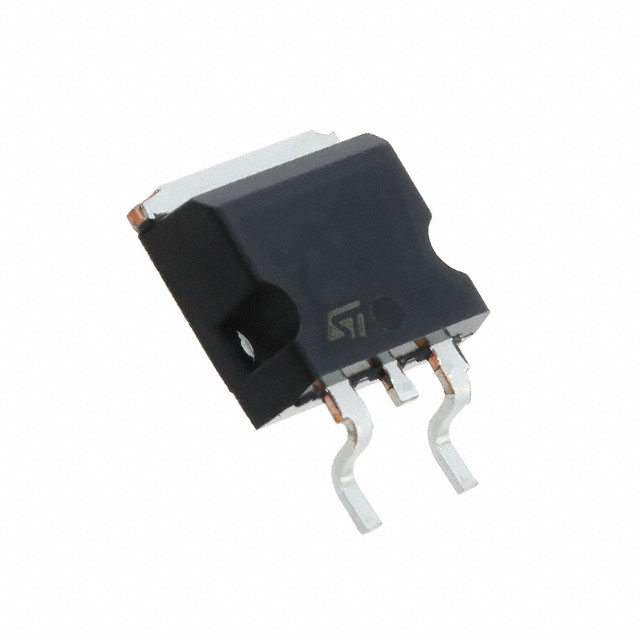
STB57N65M5

Why Choose Us?
Professional Platform
B2B & B2C purchasingDelivery at full speed
1-2 days deliveryWide variety
Original manufacturers365 days guarantee
Responsible quality
.png)


Tech Specifications
STB57N65M5 Description
STMicroelectronics' STB57N65M5 is a high-power, high-voltage MOSFET (Metal-Oxide-Semiconductor Field-Effect Transistor) designed for use in a wide range of applications. Here is a description of the model, its features, and potential applications:
Model: STB57N65M5
Description:
The STB57N65M5 is a N-channel MOSFET that offers high power density and low on-state resistance (RDS(on)). It is designed with advanced trench technology, which provides improved thermal performance and better electrical characteristics compared to traditional planar MOSFETs.
Features:
- High Voltage Rating: The device is rated for a maximum drain-source voltage (VDS) of 650V, making it suitable for high-voltage applications.
- Low On-State Resistance: With a low RDS(on) of 4.5 mΩ (typical) at a gate-source voltage (VGS) of 10V, it offers high efficiency and reduced power dissipation.
- High Power Density: The STB57N65M5 is designed to handle high power applications with its high current capability.
- Advanced Trench Technology: This technology enhances the device's thermal performance and provides better switching characteristics.
- Built-in Diode: The MOSFET features a fast-recovery, integrated body diode for efficient energy conversion in bidirectional applications.
- Robustness: The device is designed with a high level of robustness to withstand high energy pulses and transients.
Applications:
- Motor Control: The STB57N65M5 is suitable for driving high-power motors in applications like electric vehicles, industrial machinery, and pumps.
- Power Supplies: It can be used in switch-mode power supplies (SMPS) and other power conversion systems that require high efficiency and low power losses.
- Solar Energy Systems: The MOSFET's high voltage and low on-state resistance make it ideal for use in solar panel power conditioning systems.
- Battery Chargers: It can be used in high-power battery charging systems, including electric vehicle charging stations and industrial battery chargers.
- UPS Systems: The STB57N65M5 can be employed in uninterruptible power supply (UPS) systems to provide reliable power during outages or fluctuations.
- Inverters: It is suitable for use in both standalone and grid-tied inverters for converting DC power to AC power in renewable energy systems.
The STB57N65M5 is a versatile MOSFET that can be integrated into various high-power electronic systems, providing improved efficiency, reliability, and performance.
FAQ
Not available to buy online? Want the lower wholesale price? Please Send RFQ to get best price, we will respond immediately


.png?x-oss-process=image/format,webp/resize,h_32)


