
STMicroelectronics
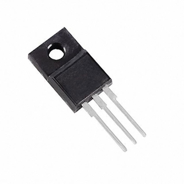
STF13N60DM2
Single FETs, MOSFETs


.png?x-oss-process=image/format,webp/resize,p_30)


STF13N60DM2 Description
STF13N60DM2 Description
The STF13N60DM2 is a high-performance N-Channel MOSFET from STMicroelectronics, designed to deliver exceptional performance in a variety of applications. With a drain-to-source voltage of 600V and a continuous drain current of 11A at 25°C, this MOSFET is ideal for high-voltage, high-current applications. The device is manufactured using advanced MOSFET technology, ensuring low on-resistance and high efficiency.
STF13N60DM2 Features
- High Voltage and Current Ratings: The STF13N60DM2 boasts a drain-to-source voltage of 600V and a continuous drain current of 11A at 25°C, making it suitable for high-voltage and high-current applications.
- Low On-Resistance: With a maximum on-resistance of 365mOhm at 5.5A and 10V, the STF13N60DM2 offers low power dissipation and high efficiency.
- Advanced MOSFET Technology: Manufactured using STMicroelectronics' advanced MOSFET technology, the STF13N60DM2 provides excellent performance and reliability.
- Wide Operating Temperature Range: The device can operate over a wide temperature range, making it suitable for various applications.
- RoHS Compliant: The STF13N60DM2 is compliant with the RoHS3 directive, making it an environmentally friendly choice.
- REACH Unaffected: The device is not affected by the REACH regulation, ensuring compliance with European chemical safety standards.
STF13N60DM2 Applications
The STF13N60DM2 is ideal for a wide range of applications, including:
- Power Supplies: Due to its high voltage and current ratings, the STF13N60DM2 is well-suited for power supply applications, such as switching power supplies and battery chargers.
- Motor Controls: The device's high current capability makes it suitable for motor control applications, including brushless DC motors and stepper motors.
- Industrial Automation: The STF13N60DM2's robust performance and reliability make it an excellent choice for industrial automation applications, such as robotic control systems and process control.
- Automotive Applications: The device's high voltage and current ratings, along with its low on-resistance, make it ideal for automotive applications, such as electric vehicle chargers and power electronics.
Conclusion of STF13N60DM2
The STF13N60DM2 is a high-performance N-Channel MOSFET from STMicroelectronics, offering exceptional performance and reliability in a variety of high-voltage and high-current applications. With its advanced MOSFET technology, low on-resistance, and compliance with environmental regulations, the STF13N60DM2 is an ideal choice for power supplies, motor controls, industrial automation, and automotive applications.
Tech Specifications
STF13N60DM2 Documents
Download datasheets and manufacturer documentation for STF13N60DM2
 Wafer 15/Feb/2019
  STF13N60DM2 Datasheet
  STF13N60DM2 Datasheet
 Shopping Guide


.png?x-oss-process=image/format,webp/resize,h_32)


