

STMicroelectronics
STF26N65DM2
Single FETs, MOSFETs

Not available to buy online? Want the lower wholesale price? Please Send RFQ to get best price, we will respond immediately


.png?x-oss-process=image/format,webp/resize,p_30)


STF26N65DM2 Description
STF26N65DM2 Description
The STF26N65DM2 is a high-performance N-Channel MOSFET from STMicroelectronics, designed for applications requiring robust power handling and efficient switching. With a drain-to-source voltage rating of 650V and a continuous drain current of 20A at 25°C, this device is well-suited for a variety of high-voltage, high-current applications.
STF26N65DM2 Features
- High Voltage Rating: Capable of handling 650V drain-to-source voltage, making it ideal for high-voltage applications.
- High Current Capability: Supports a continuous drain current of 20A at 25°C, ensuring robust power handling.
- Low On-Resistance: With a maximum Rds(on) of 190mOhm at 10A and 10V, the STF26N65DM2 offers efficient power dissipation.
- Low Gate Charge: Features a maximum gate charge (Qg) of 35.5 nC at 10V, contributing to fast switching and reduced power loss.
- Wide Gate Voltage Range: Operates with a maximum gate-source voltage (Vgs) of ±25V, providing flexibility in circuit design.
- Compliance: RoHS3 compliant and REACH unaffected, ensuring environmental and regulatory compliance.
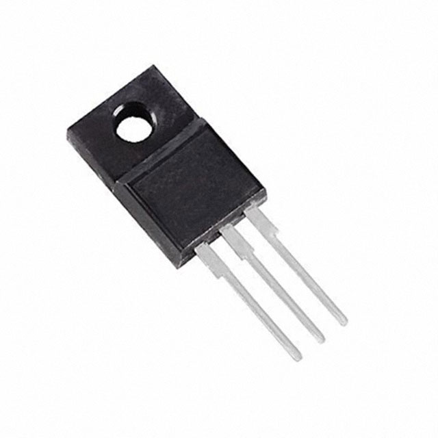
- Package: Available in a through-hole TO220FP package, facilitating easy integration into existing designs.
STF26N65DM2 Applications
The STF26N65DM2 is well-suited for a variety of applications where high voltage and current handling are required:
- Power Supplies: Ideal for high-voltage power supply designs, such as switch-mode power supplies (SMPS) and uninterruptible power supplies (UPS).
- Industrial Control: Suitable for motor control and industrial automation applications, where high voltage and current are necessary.
- Automotive: Can be used in automotive applications, such as electric vehicle (EV) charging systems and power management.
- Renewable Energy: Useful in solar power inverters and wind turbine control systems, where high-voltage and current handling are crucial.
Conclusion of STF26N65DM2
The STF26N65DM2 from STMicroelectronics is a versatile and high-performance MOSFET, offering a combination of high voltage and current ratings, low on-resistance, and fast switching capabilities. Its compliance with environmental and regulatory standards, along with its robust design, make it an excellent choice for a wide range of high-voltage and high-current applications in power electronics, industrial control, automotive, and renewable energy sectors.
Tech Specifications
STF26N65DM2 Documents
Download datasheets and manufacturer documentation for STF26N65DM2
STF26N65DM2 Related Parts


Shopping Guide


.png?x-oss-process=image/format,webp/resize,h_32)


©2025 ERSA Electronics Corporation.