
 German
 Japanese
 Portuguese
 Korea
Korea
 Mexico
 Dutch
Dutch


STMicroelectronics
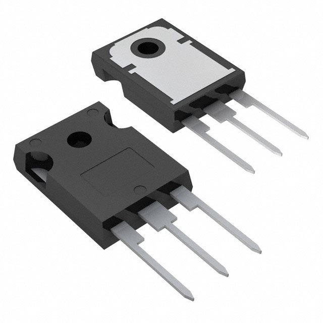
STW33N60DM2

Why Choose Us?
Professional Platform
B2B & B2C purchasingDelivery at full speed
1-2 days deliveryWide variety
Original manufacturers365 days guarantee
Responsible quality
.png)


Tech Specifications
STW33N60DM2 Description
STW33N60DM2 Description
The STW33N60DM2 is a high-performance MOSFET N-CH 600V 24A TO247 device manufactured by STMicroelectronics. This single FET is designed for applications requiring high power dissipation and efficient switching. With a maximum drain-source voltage (Vdss) of 600V and a continuous drain current (Id) of 24A at 25°C, the STW33N60DM2 offers excellent performance in demanding electronic systems.
STW33N60DM2 Features
- High Voltage and Current Ratings: The STW33N60DM2 boasts a drain-source voltage (Vdss) of 600V and a continuous drain current (Id) of 24A at 25°C, making it suitable for high-power applications.
- Low On-Resistance: With a maximum Rds(on) of 130mOhm at 12A and 10V, the STW33N60DM2 provides efficient power switching with minimal power loss.
- Fast Switching Speed: The device has a maximum gate charge (Qg) of 43nC at 10V and a threshold voltage (Vgs(th)) of 5V at 250µA, enabling fast switching and reduced switching losses.
- Robust Construction: The STW33N60DM2 is housed in a through-hole TO247 package, providing excellent thermal dissipation and mechanical stability.
- Environmental Compliance: The device is REACH unaffected and RoHS3 compliant, ensuring compliance with environmental regulations.
STW33N60DM2 Applications
The STW33N60DM2 is ideal for a variety of high-power applications, including:
- Industrial Motor Control: Due to its high voltage and current ratings, the STW33N60DM2 is well-suited for motor control applications in industrial settings.
- Power Supplies: The device's low on-resistance and fast switching capabilities make it an excellent choice for power supply designs, particularly those requiring high efficiency and low power loss.
- Automotive Electronics: The STW33N60DM2's robust construction and high power dissipation capabilities make it suitable for automotive applications, such as electric vehicle chargers and power management systems.
Conclusion of STW33N60DM2
The STW33N60DM2 is a powerful MOSFET N-CH 600V 24A TO247 device that offers excellent performance in high-power applications. Its high voltage and current ratings, low on-resistance, and fast switching capabilities make it an ideal choice for industrial motor control, power supplies, and automotive electronics. With its robust construction and environmental compliance, the STW33N60DM2 is a reliable and efficient solution for demanding electronic systems.
FAQ
Not available to buy online? Want the lower wholesale price? Please Send RFQ to get best price, we will respond immediately


.png?x-oss-process=image/format,webp/resize,h_32)


