
 German
 Japanese
 Portuguese
 Korea
Korea
 Mexico
 Dutch
Dutch


STMicroelectronics
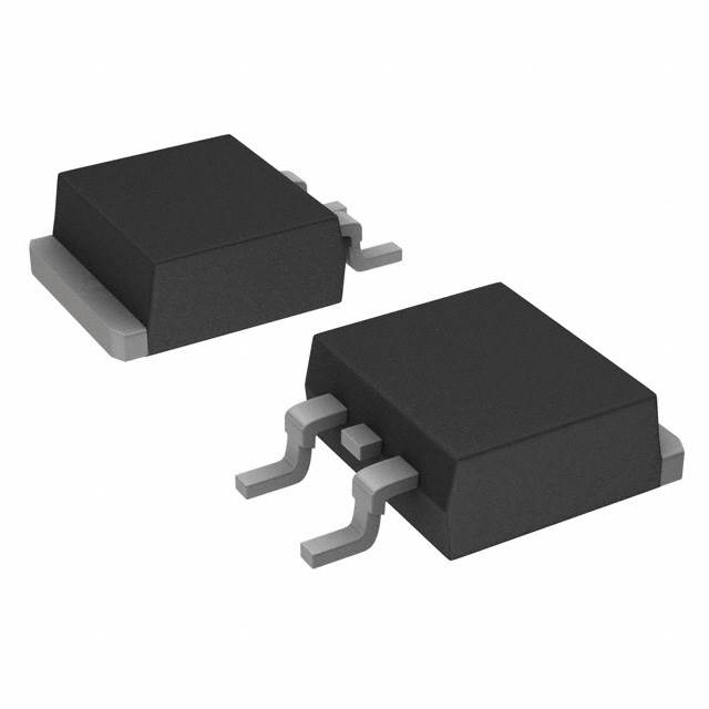
STB100NF04T4
Why Choose Us?
Professional Platform
B2B & B2C purchasingDelivery at full speed
1-2 days deliveryWide variety
Original manufacturers365 days guarantee
Responsible quality
.png)


Tech Specifications
STB100NF04T4 Description
STB100NF04T4 Description
The STB100NF04T4 from STMicroelectronics is a high-performance N-channel MOSFET designed for demanding power management applications. With a 40V drain-to-source voltage (Vdss) and 120A continuous drain current (Id), it delivers robust switching performance in a compact D2PAK (TO-263) surface-mount package. This device is part of the STripFET™ II series, leveraging advanced MOSFET (Metal Oxide) technology to achieve ultra-low on-resistance (Rds(on)) of just 4.6mΩ at 10V gate drive, ensuring minimal conduction losses. Its automotive-grade qualification makes it suitable for harsh environments, while RoHS3 compliance and REACH unaffected status ensure environmental and regulatory adherence.
STB100NF04T4 Features
- Low Rds(on): 4.6mΩ @ 50A, 10V for high efficiency and reduced heat dissipation.
- High Current Handling: 120A (Tc) continuous drain current capability.
- Fast Switching: Optimized gate charge (Qg) of 150nC @ 10V and input capacitance (Ciss) of 5100pF @ 25V for improved switching performance.
- Robust Construction: ±20V gate-source voltage (Vgs) tolerance enhances reliability in high-noise environments.
- Thermal Efficiency: 300W (Tc) power dissipation ensures stable operation under high loads.
- Automotive Grade: Meets stringent automotive standards for durability.
- Packaging: Supplied in Tape & Reel (TR) for automated assembly.
STB100NF04T4 Applications
This MOSFET is ideal for:
- DC-DC Converters: High-efficiency power conversion in industrial and automotive systems.
- Motor Control: Drives high-current motors in robotics, EVs, and industrial machinery.
- Power Supplies: Used in SMPS (Switched-Mode Power Supplies) for servers, telecom, and renewable energy systems.
- Battery Management: Enables high-current discharge protection in Li-ion battery packs.
- Automotive Systems: Suitable for LED drivers, ABS, and ignition systems due to its rugged design.
Conclusion of STB100NF04T4
The STB100NF04T4 stands out as a high-efficiency, high-current MOSFET with low conduction losses, fast switching, and automotive-grade reliability. Its optimized thermal performance and compact D2PAK package make it a top choice for power electronics engineers designing high-performance converters, motor drives, and energy-efficient systems. With STMicroelectronics' proven STripFET™ II technology, this MOSFET ensures superior performance in demanding applications.
FAQ
Not available to buy online? Want the lower wholesale price? Please Send RFQ to get best price, we will respond immediately


.png?x-oss-process=image/format,webp/resize,h_32)


