
 German
 Japanese
 Portuguese
 Korea
Korea
 Mexico
 Dutch
Dutch


STMicroelectronics
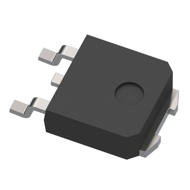
STD20NF06LAG

Why Choose Us?
Professional Platform
B2B & B2C purchasingDelivery at full speed
1-2 days deliveryWide variety
Original manufacturers365 days guarantee
Responsible quality
.png)


Tech Specifications
STD20NF06LAG Description
STD20NF06LAG Description
The STD20NF06LAG is a high-performance N-channel MOSFET from STMicroelectronics, designed for automotive applications. It features a 60V drain-to-source voltage (Vdss) and a continuous drain current (Id) of 24A at 25°C. The device is mounted on a surface mount package and is available in a tape and reel (TR) packaging. With a maximum power dissipation of 60W (Tc) and a low on-resistance (Rds On) of 40mOhm at 12A and 10V, the STD20NF06LAG offers excellent performance and efficiency.
STD20NF06LAG Features
- Technology: MOSFET (Metal Oxide)
- Series: STripFET™ II
- Input Capacitance (Ciss): 660 pF @ 25V
- Gate Charge (Qg): 13 nC @ 5V
- Drain to Source Voltage (Vdss): 60V
- Power Dissipation (Max): 60W (Tc)
- Vgs (Max): ±18V
- Rds On (Max) @ Id, Vgs: 40mOhm @ 12A, 10V
- Vgs(th) (Max) @ Id: 2.5V @ 250µA
- Current - Continuous Drain (Id) @ 25°C: 24A (Tc)
- Drive Voltage (Max Rds On, Min Rds On): 5V, 10V
- Moisture Sensitivity Level (MSL): 1 (Unlimited)
- REACH Status: REACH Unaffected
- RoHS Status: ROHS3 Compliant
- Grade: Automotive
- Mounting Type: Surface Mount
- Package: Tape & Reel (TR)
STD20NF06LAG Applications
The STD20NF06LAG's combination of high voltage, low on-resistance, and low gate charge make it ideal for a variety of automotive applications, including:
- Power Management: Efficient power conversion and distribution in automotive systems.
- Motor Control: High current and voltage ratings make it suitable for electric motor drivers.
- Battery Management: Protecting and managing battery systems in electric and hybrid vehicles.
- LED Lighting: Driving high-power LEDs in automotive lighting systems.
Conclusion of STD20NF06LAG
The STD20NF06LAG is a high-performance N-channel MOSFET designed for automotive applications. Its unique features, such as low on-resistance, low gate charge, and high voltage ratings, make it an excellent choice for power management, motor control, battery management, and LED lighting applications. With its automotive-grade qualification and compliance with REACH and RoHS regulations, the STD20NF06LAG is a reliable and efficient solution for demanding automotive electronics.
FAQ
| Quantity | Unit Price | Ext. Price |
|---|---|---|
| 1+ | $0.98228 | $0.98 |
| 10+ | $0.95828 | $9.58 |
| 30+ | $0.94115 | $28.23 |
Not available to buy online? Want the lower wholesale price? Please Send RFQ to get best price, we will respond immediately


.png?x-oss-process=image/format,webp/resize,h_32)


