
 German
 Japanese
 Portuguese
 Korea
Korea
 Mexico
 Dutch
Dutch


STMicroelectronics
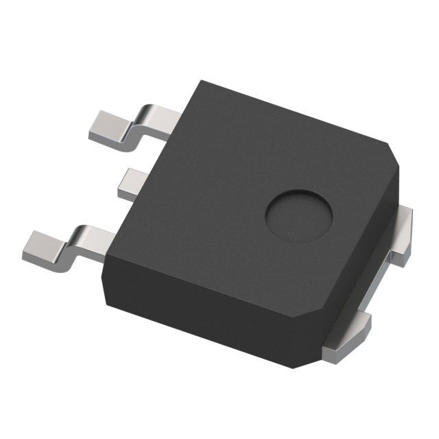
STD60NF55LAT4

Why Choose Us?
Professional Platform
B2B & B2C purchasingDelivery at full speed
1-2 days deliveryWide variety
Original manufacturers365 days guarantee
Responsible quality
.png)


Tech Specifications
STD60NF55LAT4 Description
STD60NF55LAT4 Description
The STD60NF55LAT4 is a high-performance, automotive-grade N-channel MOSFET manufactured by STMicroelectronics. This device is designed for demanding applications that require high efficiency and reliability. With a drain-to-source voltage (Vdss) of 55V and a continuous drain current (Id) of 60A at 25°C, the STD60NF55LAT4 is capable of handling high power levels while maintaining low on-resistance (Rds On) of 15mOhm at 30A and 10V. The device is also designed to operate over a wide range of gate-source voltages (Vgs), with a maximum of ±15V.
STD60NF55LAT4 Features
- High Drain-to-Source Voltage (Vdss): 55V, enabling the device to handle high voltage applications.
- Continuous Drain Current (Id): 60A at 25°C, providing high current capacity.
- Low On-Resistance (Rds On): 15mOhm at 30A and 10V, reducing power losses and improving efficiency.
- Wide Gate-Source Voltage Range (Vgs): ±15V, offering flexibility in gate drive requirements.
- SuperFET® II Series: Known for its superior performance and reliability in automotive applications.
- Automotive Grade: Designed to meet the stringent requirements of automotive electronics.
- Surface Mount Technology:。
- REACH Unaffected and RoHS3 Compliant: Ensuring environmental compliance and reducing the risk of regulatory issues.
STD60NF55LAT4 Applications
The STD60NF55LAT4 is ideal for a variety of high-power applications in the automotive sector, including:
- Electric Vehicle (EV) Systems: Such as battery management systems, motor controls, and power inverters.
- Power Management Systems: For managing high current and voltage in automotive electronics.
- Industrial Control Systems: Where high power and reliability are crucial.
- High-End Audio Amplifiers: Due to its ability to handle high current and provide low distortion.
Conclusion of STD60NF55LAT4
The STD60NF55LAT4 stands out in the market for its combination of high voltage and current handling capabilities, low on-resistance, and automotive-grade reliability. Its unique features make it an excellent choice for demanding applications where performance and durability are critical. With its compliance with environmental regulations and its robust design, the STD60NF55LAT4 is a reliable component for engineers looking to build high-performance automotive and industrial systems.
FAQ
Not available to buy online? Want the lower wholesale price? Please Send RFQ to get best price, we will respond immediately


.png?x-oss-process=image/format,webp/resize,h_32)


