

STMicroelectronics
STF19NM50N
Single FETs, MOSFETs

Not available to buy online? Want the lower wholesale price? Please Send RFQ to get best price, we will respond immediately


.png?x-oss-process=image/format,webp/resize,p_30)


STF19NM50N Description
STF19NM50N Description
The STF19NM50N is a high-performance N-Channel MOSFET from STMicroelectronics, designed for applications requiring high voltage and current capabilities. With a drain-to-source voltage (Vdss) of 500V and a continuous drain current (Id) of 14A at 25°C, this MOSFET is suitable for a wide range of power electronics applications.
STF19NM50N Features
- High Voltage and Current Ratings: The STF19NM50N boasts a drain-to-source voltage (Vdss) of 500V and a continuous drain current (Id) of 14A at 25°C, making it ideal for high-power applications.
- Low On-Resistance: With a maximum Rds(on) of 250mOhm at 7A and 10V, the STF19NM50N offers low power dissipation and high efficiency.
- Robust Gate Drive: The device features a maximum gate-source voltage (Vgs) of ±25V, ensuring reliable operation in various gate drive circuits.
- Low Gate Charge: The maximum gate charge (Qg) is 34nC at 10V, contributing to fast switching speeds and low switching losses.
- Thermal Performance: The STF19NM50N has a maximum power dissipation of 30W (Tc) and an operating junction temperature (TJ) of 150°C, ensuring reliable operation in high-temperature environments.
- Environmental Compliance: The device is REACH unaffected and RoHS3 compliant, making it suitable for environmentally conscious applications.
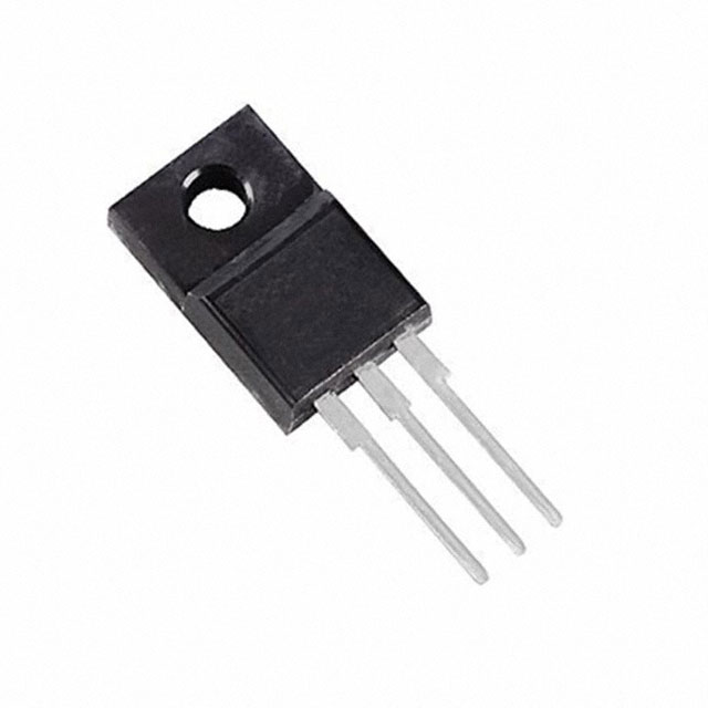
- Mounting Type: The STF19NM50N is available in a through-hole TO220FP package, providing a robust and reliable mechanical connection.
STF19NM50N Applications
The STF19NM50N is ideal for a variety of power electronics applications, including:
- Power Supplies: The high voltage and current ratings make it suitable for use in power supply designs, such as switch-mode power supplies (SMPS) and uninterruptible power supplies (UPS).
- Motor Control: The low on-resistance and fast switching capabilities make the STF19NM50N an excellent choice for motor control applications, including brushless DC (BLDC) motors and stepper motors.
- Industrial Automation: The device's robust performance and environmental compliance make it suitable for use in industrial automation systems, such as robotic arms and conveyor systems.
- Automotive Applications: The STF19NM50N can be used in various automotive applications, including electric vehicle (EV) charging systems, battery management systems, and power window controls.
Conclusion of STF19NM50N
The STF19NM50N from STMicroelectronics is a high-performance N-Channel MOSFET designed for demanding power electronics applications. Its combination of high voltage and current ratings, low on-resistance, and robust thermal performance make it an ideal choice for a wide range of applications, including power supplies, motor control, industrial automation, and automotive systems. With its environmental compliance and reliable mechanical connection, the STF19NM50N is a versatile and dependable solution for engineers designing high-performance electronic systems.
Tech Specifications
STF19NM50N Documents
Download datasheets and manufacturer documentation for STF19NM50N
STx19NM50N STF19NM50N View All Specifications STx19NM50N Related Parts


Shopping Guide


.png?x-oss-process=image/format,webp/resize,h_32)


©2025 ERSA Electronics Corporation.