
 German
 Japanese
 Portuguese
 Korea
Korea
 Mexico
 Dutch
Dutch


STMicroelectronics
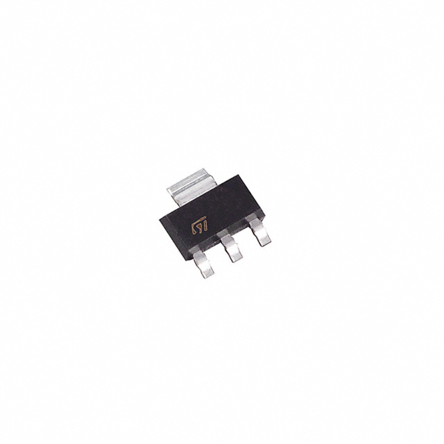
STN3P6F6

Why Choose Us?
Professional Platform
B2B & B2C purchasingDelivery at full speed
1-2 days deliveryWide variety
Original manufacturers365 days guarantee
Responsible quality
.png)


Tech Specifications
STN3P6F6 Description
STN3P6F6 Description
The STN3P6F6 is a high-performance P-Channel MOSFET from STMicroelectronics, designed to deliver superior performance in various electronic applications. This MOSFET features a drain-to-source voltage (Vdss) of 60V, making it suitable for high-voltage applications. With a maximum power dissipation of 2.6W (Tc), the STN3P6F6 can handle demanding power requirements. Its low gate charge (Qg) of 6.4 nC @ 10V and low input capacitance (Ciss) of 340 pF @ 48V contribute to its fast switching capabilities, making it ideal for high-frequency applications.
STN3P6F6 Features
- DeepGATE™, STripFET™ VI Series: The STN3P6F6 belongs to the DeepGATE™, STripFET™ VI series, which is known for its excellent performance and reliability.
- Low Rds On: With a maximum Rds On of 160mOhm @ 1.5A, 10V, the STN3P6F6 offers low on-resistance, reducing power loss and improving efficiency.
- High Input Capacitance: The 340 pF @ 48V input capacitance ensures fast switching and high-frequency operation.
- Low Gate Charge: The 6.4 nC @ 10V gate charge enables fast switching and reduces power consumption.
- Robust Voltage Ratings: The STN3P6F6 can handle a maximum Vgs of ±20V and a Vdss of 60V, making it suitable for high-voltage applications.
- Compliance: The STN3P6F6 is REACH unaffected, RoHS3 compliant, and moisture sensitivity level 1 (unlimited), ensuring environmental and regulatory compliance.
STN3P6F6 Applications
The STN3P6F6 is ideal for a wide range of applications, including:
- Power Management: Due to its high voltage and power ratings, the STN3P6F6 is suitable for power management applications in various electronic devices.
- Motor Control: Its low Rds On and high Vdss make it an excellent choice for motor control applications, providing efficient power switching and control.
- Automotive Electronics: The STN3P6F6 can be used in automotive electronics, such as power windows, seat controls, and other high-voltage applications.
- Industrial Control: Its robust voltage ratings and fast switching capabilities make it suitable for industrial control applications, such as motor drives and power supplies.
Conclusion of STN3P6F6
The STN3P6F6 is a high-performance P-Channel MOSFET from STMicroelectronics, offering excellent technical specifications and performance benefits. Its low Rds On, high input capacitance, and low gate charge make it ideal for high-frequency and high-voltage applications. With its compliance to various environmental and regulatory standards, the STN3P6F6 is a reliable choice for a wide range of applications, including power management, motor control, automotive electronics, and industrial control.
FAQ
| Quantity | Unit Price | Ext. Price |
|---|---|---|
| 1+ | $0.74743 | $0.75 |
| 10+ | $0.60857 | $6.09 |
| 30+ | $0.53828 | $16.15 |
| 100+ | $0.46972 | $46.97 |
| 500+ | $0.41143 | $205.72 |
Not available to buy online? Want the lower wholesale price? Please Send RFQ to get best price, we will respond immediately


.png?x-oss-process=image/format,webp/resize,h_32)


