
 German
 Japanese
 Portuguese
 Korea
Korea
 Mexico
 Dutch
Dutch


STMicroelectronics
STL9N60M2

Why Choose Us?
Professional Platform
B2B & B2C purchasingDelivery at full speed
1-2 days deliveryWide variety
Original manufacturers365 days guarantee
Responsible quality
.png)


Tech Specifications
STL9N60M2 Description
STL9N60M2 Description
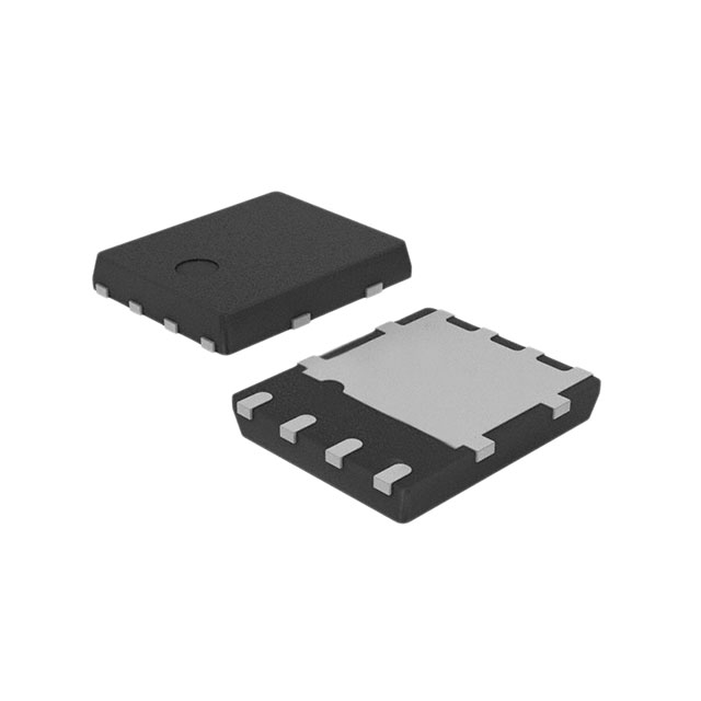
The STL9N60M2 is a high-performance N-Channel MOSFET from STMicroelectronics, designed for power electronics applications. It is part of the MDmesh™ II Plus series and offers a superior combination of high voltage and low on-resistance. The device is manufactured using advanced MOSFET technology and is available in a PowerFlat™ (5x6) HV package, making it suitable for surface mount applications.
STL9N60M2 Features
- High Voltage Rating: The STL9N60M2 can handle drain-to-source voltages up to 600V, making it ideal for high-voltage applications.
- Low On-Resistance: With a maximum on-resistance of 860mOhm at 2.4A and 10V, the device offers high efficiency and low power dissipation.
- High Input Capacitance: The maximum input capacitance is 320 pF at 100V, ensuring fast switching speeds and low gate charge.
- Robust Gate Drive: The device can handle gate-source voltages up to ±25V, providing flexibility in gate drive requirements.
- Low Threshold Voltage: The maximum threshold voltage is 4V at 250µA, enabling easy turn-on and low drive current.
- Power Dissipation: The maximum power dissipation is 48W at case temperature, ensuring reliable operation in high-power applications.
- Operating Temperature: The device can operate at junction temperatures up to 150°C, making it suitable for high-temperature environments.
- Compliance: The STL9N60M2 is compliant with RoHS3 and REACH regulations, ensuring environmental and safety standards are met.
STL9N60M2 Applications
The STL9N60M2 is ideal for a wide range of power electronics applications, including:
- Power Supplies: The high voltage and low on-resistance make it suitable for power supply designs, such as SMPS and DC-DC converters.
- Motor Control: The device's high current capability and low on-resistance make it ideal for motor control applications, including industrial drives and electric vehicles.
- Renewable Energy: The high voltage rating and robustness make it suitable for renewable energy applications, such as solar inverters and wind power systems.
- Industrial Automation: The device's high power dissipation and operating temperature range make it ideal for industrial automation applications, including motor drives and power distribution.
Conclusion of STL9N60M2
The STL9N60M2 is a high-performance N-Channel MOSFET that offers a unique combination of high voltage, low on-resistance, and robust performance. Its advanced features, such as high input capacitance and low threshold voltage, make it an ideal choice for a wide range of power electronics applications. With its compliance with RoHS3 and REACH regulations, the STL9N60M2 is a reliable and environmentally friendly solution for demanding power electronics designs.
FAQ
Not available to buy online? Want the lower wholesale price? Please Send RFQ to get best price, we will respond immediately


.png?x-oss-process=image/format,webp/resize,h_32)


