
 German
 Japanese
 Portuguese
 Korea
Korea
 Mexico
 Dutch
Dutch


STMicroelectronics
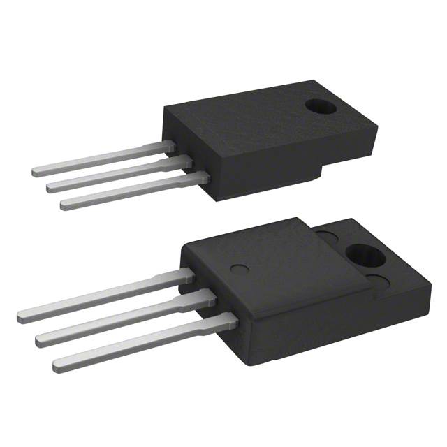
STF24N60M2

Why Choose Us?
Professional Platform
B2B & B2C purchasingDelivery at full speed
1-2 days deliveryWide variety
Original manufacturers365 days guarantee
Responsible quality
.png)


Tech Specifications
STF24N60M2 Description
The STF24N60M2 is a high voltage N-channel MOSFET from STMicroelectronics. It is designed for use in a variety of applications, including motor control, power supplies, and power converters.
Description:
The STF24N60M2 is a high voltage N-channel MOSFET that features a drain-source voltage (VDS) of 600V and a continuous drain current (ID) of 2.4A. It has a low on-state resistance (RDS(on)) of 0.085 ohms maximum at a gate-source voltage (VGS) of 10V. The device also has a fast switching speed and low gate charge, making it suitable for use in high efficiency power conversion applications.
Features:
- High drain-source voltage (VDS) of 600V
- Continuous drain current (ID) of 2.4A
- Low on-state resistance (RDS(on)) of 0.085 ohms maximum at VGS of 10V
- Fast switching speed and low gate charge
- Suitable for use in high efficiency power conversion applications
Applications:
- Motor control
- Power supplies
- Power converters
- High voltage switching applications
The STF24N60M2 is available in a variety of packages, including a TO-220 package and a DPAK package. It is designed to operate over a wide range of temperatures, making it suitable for use in a variety of environments. The device is also RoHS compliant, making it suitable for use in environmentally friendly applications.
FAQ
| Quantity | Unit Price | Ext. Price |
|---|---|---|
| 1+ | $1.20685 | $1.21 |
| 10+ | $0.97715 | $9.77 |
| 50+ | $0.86400 | $43.20 |
Not available to buy online? Want the lower wholesale price? Please Send RFQ to get best price, we will respond immediately


.png?x-oss-process=image/format,webp/resize,h_32)


