
 German
 Japanese
 Portuguese
 Korea
Korea
 Mexico
 Dutch
Dutch


STMicroelectronics
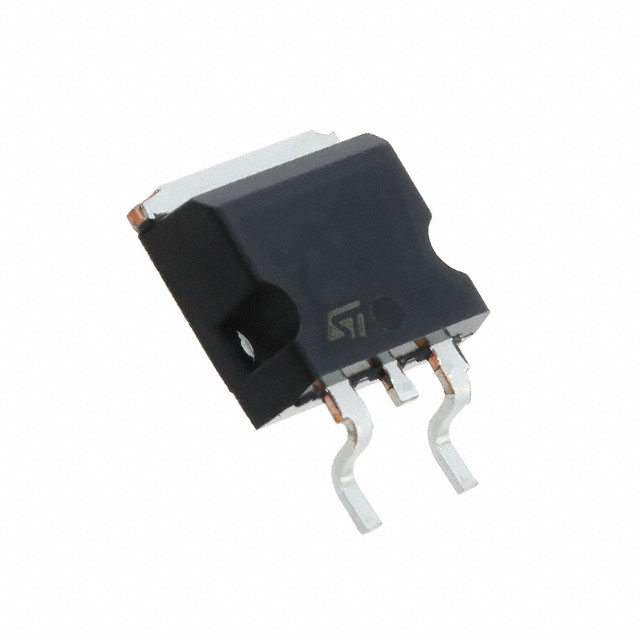
STB10N60M2

Why Choose Us?
Professional Platform
B2B & B2C purchasingDelivery at full speed
1-2 days deliveryWide variety
Original manufacturers365 days guarantee
Responsible quality
.png)


Tech Specifications
STB10N60M2 Description
STB10N60M2 Description
The STB10N60M2 from STMicroelectronics is a high-performance N-channel 600V, 7.5A power MOSFET designed for demanding switching applications. Part of the MDmesh™ II Plus series, it leverages advanced Metal Oxide (MOSFET) technology to deliver superior efficiency, low conduction losses, and high switching speed. With a low on-resistance (Rds(on)) of 600mΩ at 10V gate drive, it minimizes power dissipation, making it ideal for high-voltage, high-frequency circuits. The device is housed in a D2PAK (TO-263) surface-mount package, ensuring robust thermal performance and compatibility with automated assembly processes.
STB10N60M2 Features
- High Voltage Rating: 600V Vdss ensures reliability in high-power applications.
- Low Gate Charge (Qg): 13.5nC @ 10V reduces switching losses, enhancing efficiency.
- Optimized Rds(on): 600mΩ @ 3A, 10V for minimal conduction losses.
- Fast Switching: Low input capacitance (Ciss = 400pF @ 100V) enables high-frequency operation.
- Robust Gate Drive: ±25V Vgs(max) tolerance for flexible drive circuitry.
- Thermal Efficiency: 85W power dissipation (Tc) ensures stable performance under load.
- Reliability: ROHS3 compliant, REACH unaffected, and MSL 1 (unlimited) for environmental and handling robustness.
STB10N60M2 Applications
The STB10N60M2 excels in:
- Switch-Mode Power Supplies (SMPS): High efficiency and fast switching make it ideal for AC-DC converters.
- Motor Drives: Low Rds(on) and high voltage tolerance suit inverter and H-bridge designs.
- Lighting Systems: Efficiently drives LED drivers and ballasts.
- Industrial Power Systems: Used in welding equipment, UPS, and solar inverters.
- Automotive Applications: Suitable for auxiliary power systems where high voltage and reliability are critical.
Conclusion of STB10N60M2
The STB10N60M2 stands out as a high-efficiency, high-voltage MOSFET with low switching losses and robust thermal performance. Its MDmesh™ II Plus technology ensures superior performance in power conversion applications, while the D2PAK package offers mechanical and thermal advantages. Whether in industrial, automotive, or consumer electronics, this MOSFET delivers reliability, efficiency, and flexibility, making it a top choice for designers prioritizing performance and cost-effectiveness.
FAQ
Not available to buy online? Want the lower wholesale price? Please Send RFQ to get best price, we will respond immediately


.png?x-oss-process=image/format,webp/resize,h_32)


