
STMicroelectronics
STP40N65M2
Single FETs, MOSFETs


.png?x-oss-process=image/format,webp/resize,p_30)


STP40N65M2 Description
STP40N65M2 Description
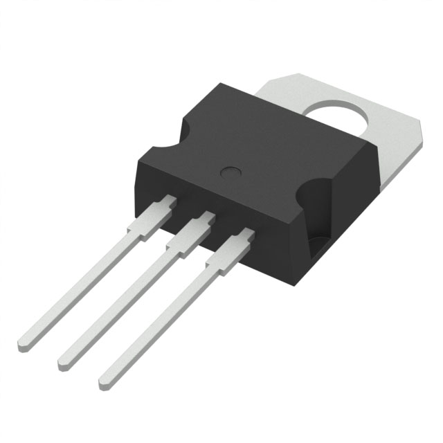
The STP40N65M2 is a high-performance MOSFET (Metal Oxide) from STMicroelectronics, designed for applications requiring high voltage and current capabilities. This N-Channel MOSFET operates at a drain-to-source voltage of 650V and can handle continuous drain currents of up to 32A at 25°C. With a maximum power dissipation of 250W, the STP40N65M2 is well-suited for demanding applications in the electronics industry.
STP40N65M2 Features
- High Voltage and Current Ratings: The STP40N65M2 boasts a drain-to-source voltage of 650V and can handle continuous drain currents of up to 32A at 25°C, making it ideal for high-power applications.
- Low On-Resistance: With a maximum on-resistance (Rds(on)) of 99mOhm at 16A and 10V, the STP40N65M2 offers efficient power dissipation and reduced power losses.
- Robust Gate Charge and Input Capacitance: The device features a maximum gate charge (Qg) of 56.5nC at 10V and an input capacitance (Ciss) of 2355pF at 100V, ensuring fast switching and minimal parasitic effects.
- Compliance and Environmental Standards: The STP40N65M2 is REACH unaffected and RoHS3 compliant, adhering to strict environmental and safety regulations.
- Wide Operating Temperature Range: The device operates within a junction temperature range of -55°C to 150°C, making it suitable for a variety of applications in different environmental conditions.
STP40N65M2 Applications
The STP40N65M2 is an ideal choice for applications requiring high voltage and current capabilities, such as:
- Power Supplies: The high voltage and current ratings make it suitable for power supply designs, including switching power supplies and battery chargers.
- Industrial Control Systems: The robust performance and compliance with environmental standards make it ideal for use in industrial control systems, where reliability and safety are paramount.
- Automotive Applications: The STP40N65M2's high voltage and temperature ratings make it suitable for automotive applications, such as electric vehicle charging systems and power electronics.
Conclusion of STP40N65M2
The STP40N65M2 from STMicroelectronics is a high-performance MOSFET that offers a combination of high voltage and current ratings, low on-resistance, and compliance with environmental standards. Its robust performance and wide operating temperature range make it an ideal choice for a variety of applications in the electronics industry, including power supplies, industrial control systems, and automotive applications. With its unique features and advantages over similar models, the STP40N65M2 is a reliable and efficient solution for demanding applications.
Tech Specifications
STP40N65M2 Documents
Download datasheets and manufacturer documentation for STP40N65M2
 ST(I,P)40N65M2
  ST(I,P)40N65M2
 Shopping Guide


.png?x-oss-process=image/format,webp/resize,h_32)


