

STMicroelectronics
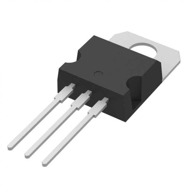
STP45NF06
Single FETs, MOSFETs

Not available to buy online? Want the lower wholesale price? Please Send RFQ to get best price, we will respond immediately


.png?x-oss-process=image/format,webp/resize,p_30)


STP45NF06 Description
STP45NF06 Description
The STP45NF06 is a high-performance N-Channel MOSFET from STMicroelectronics, designed for demanding applications requiring high power dissipation and low on-resistance. With a drain-to-source voltage of 60V and a continuous drain current of 38A at 25°C, this device is well-suited for applications such as motor control, power supplies, and industrial electronics.
STP45NF06 Features
- Technology: Advanced MOSFET (Metal Oxide) technology for high efficiency and reliability.
- Low On-Resistance: Maximum Rds(on) of 28mOhm at 19A and 10V, ensuring minimal power loss.
- High Input Capacitance: Maximum Ciss of 980 pF at 25V, reducing switching losses and improving performance.
- Gate Charge: Maximum Qg of 58 nC at 10V, enabling fast switching speeds.
- Robust Voltage Ratings: Maximum Vgs of ±20V and Vdss of 60V for reliable operation in high-voltage environments.
- Thermal Performance: Power dissipation up to 80W (Tc) and operating temperature up to 175°C (TJ), making it suitable for high-power applications.
- Mounting Type: Through-hole mounting in a TO220AB package, providing easy integration into existing designs.
- Compliance: REACH Unaffected, ROHS3 Compliant, and Moisture Sensitivity Level 1, ensuring environmental and regulatory compliance.
STP45NF06 Applications
The STP45NF06 is ideal for a wide range of applications where high power handling, low on-resistance, and robust voltage ratings are critical:
- Motor Control: Efficiently drives high-power motors in industrial and automotive applications.
- Power Supplies: Provides high-efficiency power conversion in switch-mode power supplies (SMPS) and uninterruptible power supplies (UPS).
- Industrial Electronics: Reliable operation in harsh environments with high power dissipation and temperature requirements.
- Automotive: Used in various automotive systems, such as electric power steering (EPS) and battery management systems.
Conclusion of STP45NF06
The STP45NF06 from STMicroelectronics offers a powerful combination of high voltage, low on-resistance, and robust thermal performance, making it an excellent choice for demanding high-power applications. Its advanced MOSFET technology, compliance with environmental and regulatory standards, and versatile mounting options make it a preferred choice for engineers designing cutting-edge electronic systems.
Tech Specifications
STP45NF06 Documents
Download datasheets and manufacturer documentation for STP45NF06
TO-220 ECOPACK 2 graded moulding compound assembly capacity expansion - Subcontractor PSI Laguna (Philippines) (PDF) Product / Process Change Notification (PDF) Product Change Notification (PDF) Product Change Notification 2024-04-04 (PDF) PRODUCT CHANGE NOTIFICATION (PDF) Related Parts


Shopping Guide


.png?x-oss-process=image/format,webp/resize,h_32)


©2025 ERSA Electronics Corporation.