

STMicroelectronics
STB28N60DM2
Single FETs, MOSFETs

Not available to buy online? Want the lower wholesale price? Please Send RFQ to get best price, we will respond immediately


.png?x-oss-process=image/format,webp/resize,p_30)


STB28N60DM2 Description
STB28N60DM2 is a high voltage N-channel MOSFET transistor manufactured by STMicroelectronics. It is designed for use in a variety of applications, including high voltage switching and power management.
Description:
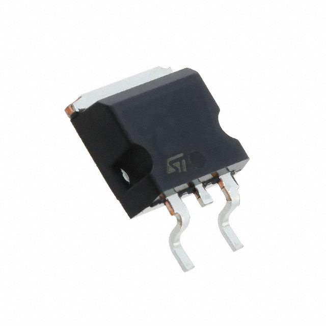
The STB28N60DM2 is an N-channel enhancement mode field effect transistor (MOSFET). It is a three-pin device, with a source (S), drain (D), and gate (G) terminal. The device is available in a TO-220 package.
Features:
- High voltage operation: The STB28N60DM2 is rated for a maximum drain-source voltage (VDS) of 600V, making it suitable for use in high voltage applications.
- High current capability: The device can handle a continuous drain current (ID) of up to 28A, making it suitable for use in high current applications.
- Low on-state resistance (RDS(on)): The STB28N60DM2 has a low on-state resistance (RDS(on)) of 0.65 ohms (maximum) at a gate-source voltage (VGS) of 10V, which helps to minimize power dissipation in the device.
- Fast switching speed: The device has a fast switching speed, with a typical gate charge (Qg) of 46nC and a typical turn-on delay time (td(on)) of 4.6ns.
Applications:
The STB28N60DM2 is suitable for use in a variety of applications, including:
- High voltage switching: The device's high voltage rating makes it suitable for use in high voltage switching applications, such as in power supplies and motor control circuits.
- Power management: The STB28N60DM2 can be used in power management applications, such as in battery chargers and power adapters.
- Motor control: The device's high current capability and fast switching speed make it suitable for use in motor control applications, such as in industrial machinery and automotive systems.
In summary, the STB28N60DM2 is a high voltage, high current N-channel MOSFET transistor that offers fast switching speed and low on-state resistance. It is suitable for use in a variety of high voltage and high current applications, including high voltage switching, power management, and motor control.
Tech Specifications
STB28N60DM2 Documents
Download datasheets and manufacturer documentation for STB28N60DM2
Wafer 15/Feb/2019 ST(B,P,W)28N60DM2 Mult Dev Inner Box Chg 9/Dec/2021 ST(B,P,W)28N60DM2 Related Parts


Shopping Guide


.png?x-oss-process=image/format,webp/resize,h_32)


©2025 ERSA Electronics Corporation.