

STMicroelectronics
STL7N6F7
Single FETs, MOSFETs

Not available to buy online? Want the lower wholesale price? Please Send RFQ to get best price, we will respond immediately


.png?x-oss-process=image/format,webp/resize,p_30)


STL7N6F7 Description
STL7N6F7 Description
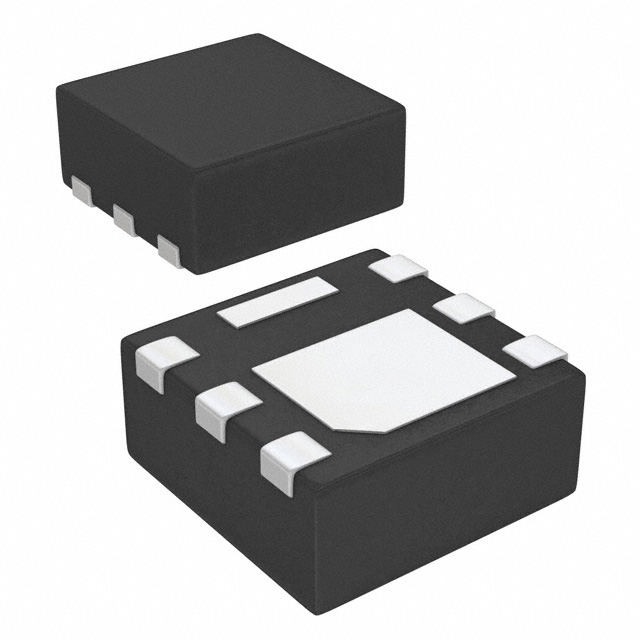
The STL7N6F7 is a high-performance N-Channel MOSFET from STMicroelectronics, designed for applications requiring efficient power management and control. It features a 60V drain-to-source voltage rating and can handle continuous drain currents up to 7A at 25°C. The device is housed in a compact PowerFlat™ (2x2) package, making it ideal for space-constrained applications.
STL7N6F7 Features
-
Technical Specifications:
- Input Capacitance (Ciss): 450 pF @ 25 V
- Gate Charge (Qg): 8 nC @ 10 V
- Drain to Source Voltage (Vdss): 60 V
- Power Dissipation (Max): 2.4W (Ta)
- Technology: MOSFET (Metal Oxide)
- Vgs (Max): ±20V
- Rds On (Max) @ Id, Vgs: 25mOhm @ 3.5A, 10V
- Vgs(th) (Max) @ Id: 4V @ 250µA
- Current - Continuous Drain (Id) @ 25°C: 7A (Tc)
- Drive Voltage (Max Rds On, Min Rds On): 10V
-
Performance Benefits:
- Low Rds On (25mOhm) for high efficiency
- Low gate charge (8 nC) for fast switching
- Robust 60V drain-to-source voltage rating
-
Unique Features and Advantages:
- STripFET™ series for improved performance and reliability
- REACH Unaffected and ROHS3 Compliant for environmental compliance
- Moisture Sensitivity Level (MSL) 1 for unlimited storage time
STL7N6F7 Applications
The STL7N6F7 is ideal for a variety of applications where efficient power management and control are critical:
-
Power Management: In power supply designs, battery management systems, and motor control applications, the STL7N6F7's low Rds On and high drain current capabilities ensure efficient power delivery and control.
-
Automotive Applications: The device's robust voltage rating and low gate charge make it suitable for automotive applications such as electric vehicle (EV) charging systems and in-vehicle power management.
-
Industrial Control: In industrial control systems, the STL7N6F7 can be used for motor drives, power conversion, and other high-power applications where reliability and efficiency are paramount.
Conclusion of STL7N6F7
The STL7N6F7 from STMicroelectronics is a versatile and high-performance N-Channel MOSFET designed for demanding power management applications. Its unique combination of low Rds On, high drain current, and robust voltage rating make it an excellent choice for power supply designs, automotive systems, and industrial control applications. With its REACH Unaffected and ROHS3 Compliant status, the STL7N6F7 is also an environmentally responsible choice for your next project.
Tech Specifications
STL7N6F7 Documents
Download datasheets and manufacturer documentation for STL7N6F7
Product Change Notification 2024-05-20 (PDF) Product Change Notification (PDF) Related Parts


Shopping Guide


.png?x-oss-process=image/format,webp/resize,h_32)


©2025 ERSA Electronics Corporation.