
 German
 Japanese
 Portuguese
 Korea
Korea
 Mexico
 Dutch
Dutch


STMicroelectronics
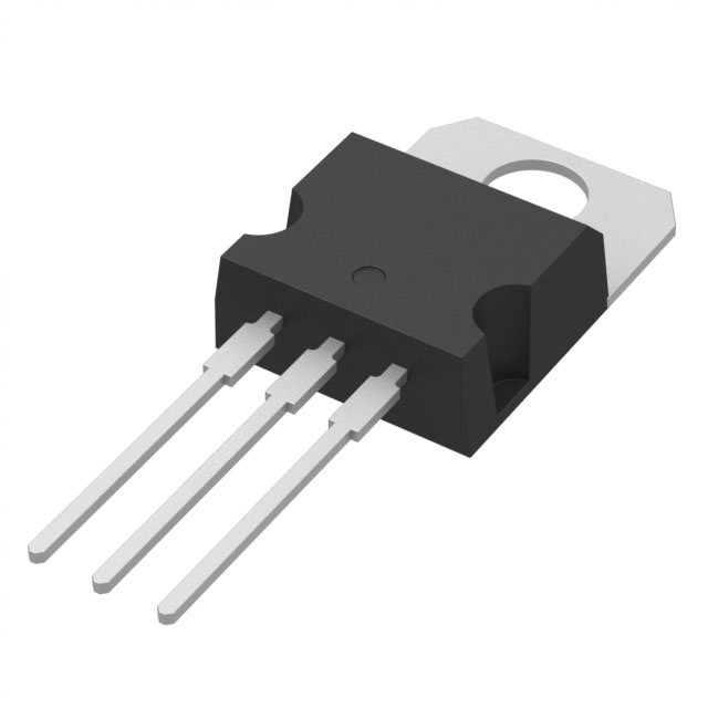
STP28N65M2

Why Choose Us?
Professional Platform
B2B & B2C purchasingDelivery at full speed
1-2 days deliveryWide variety
Original manufacturers365 days guarantee
Responsible quality
.png)


Tech Specifications
STP28N65M2 Description
STP28N65M2 Description
The STP28N65M2 is a high-performance N-Channel MOSFET from STMicroelectronics, designed for applications requiring high voltage and current handling capabilities. With a drain-to-source voltage of 650V and a continuous drain current of 20A at 25°C, this device is well-suited for demanding power electronics applications. The STP28N65M2 features a low on-resistance of 180mOhm at 10A and 10V, ensuring efficient power dissipation and minimizing power losses.
STP28N65M2 Features
- 650V Drain-to-Source Voltage (Vdss): Capable of handling high voltage applications.
- 20A Continuous Drain Current (Id): High current capacity for power electronics.
- 180mOhm On-Resistance (Rds On): Low resistance for efficient power dissipation.
- 35nC Maximum Gate Charge (Qg): Minimizes power losses in the gate drive circuit.
- 1440pF Maximum Input Capacitance (Ciss): Facilitates high-speed switching.
- 4V Maximum Threshold Voltage (Vgs(th)): Ensures reliable device turn-on.
- 10V Maximum Drive Voltage: Compatible with various gate drive circuits.
- 170W Maximum Power Dissipation (Tc): Suitable for high-power applications.
- 150°C Maximum Operating Temperature (TJ): Designed for high-temperature environments.
- ROHS3 Compliance: Environmentally friendly and suitable for green electronics.
- REACH Unaffected Status: Compliant with European chemical regulations.
STP28N65M2 Applications
The STP28N65M2 is ideal for a variety of power electronics applications, including:
- Power Supplies: High-efficiency power conversion in switch-mode power supplies (SMPS).
- Motor Controls: Reliable and efficient motor drive in industrial and automotive applications.
- Inverters: High-voltage and high-current handling in solar and electric vehicle inverters.
- Battery Management Systems: Efficient battery charging and protection in energy storage systems.
Conclusion of STP28N65M2
The STP28N65M2 from STMicroelectronics is a high-performance N-Channel MOSFET designed for demanding power electronics applications. Its combination of high voltage and current ratings, low on-resistance, and compliance with environmental regulations make it an excellent choice for power supplies, motor controls, inverters, and battery management systems. With its robust performance and unique features, the STP28N65M2 offers a reliable and efficient solution for high-power applications.
FAQ
| Quantity | Unit Price | Ext. Price |
|---|---|---|
| 1+ | $6.94800 | $6.95 |
| 10+ | $6.02743 | $60.27 |
| 30+ | $5.46685 | $164.01 |
Not available to buy online? Want the lower wholesale price? Please Send RFQ to get best price, we will respond immediately


.png?x-oss-process=image/format,webp/resize,h_32)


