
 German
 Japanese
 Portuguese
 Korea
Korea
 Mexico
 Dutch
Dutch


STMicroelectronics
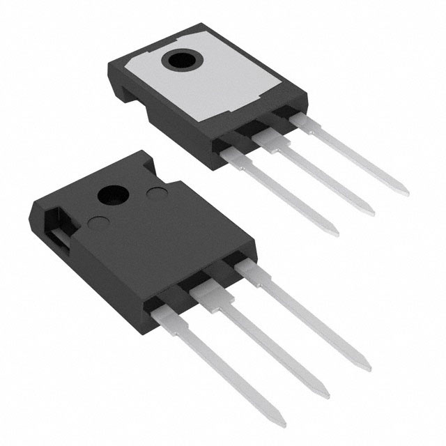
STWA40N90K5

Why Choose Us?
Professional Platform
B2B & B2C purchasingDelivery at full speed
1-2 days deliveryWide variety
Original manufacturers365 days guarantee
Responsible quality
.png)


Tech Specifications
STWA40N90K5 Description
STWA40N90K5 Description
The STWA40N90K5 is a high-performance MOSFET (Metal Oxide) from STMicroelectronics, designed for applications requiring robust power handling and efficient switching. With a drain to source voltage (Vdss) of 900V and a continuous drain current (Id) of 40A at 25°C, this device is ideal for high-voltage, high-current applications.
STWA40N90K5 Features
- High Voltage and Current Ratings: The STWA40N90K5 boasts a drain to source voltage (Vdss) of 900V and a continuous drain current (Id) of 40A at 25°C, making it suitable for demanding power electronics applications.
- Low On-Resistance: The device features a maximum on-resistance (Rds On) of 99mOhm at 20A and 10V, ensuring efficient power dissipation and reduced power loss.
- Robust Gate Drive: With a maximum gate-source voltage (Vgs) of ±30V, the STWA40N90K5 can handle a wide range of gate drive voltages, providing flexibility in circuit design.
- Low Gate Charge: A maximum gate charge (Qg) of 89nC at 10V reduces switching losses and improves efficiency in high-frequency applications.
- Reliability and Compliance: The STWA40N90K5 is compliant with REACH and RoHS3 regulations, ensuring environmental and safety compliance. It also features a moisture sensitivity level (MSL) of 1, allowing for unlimited storage time without baking.
STWA40N90K5 Applications
The STWA40N90K5 is ideal for a variety of high-voltage, high-current applications, including:
- Power Supplies: The high voltage and current ratings make it suitable for power supply designs, particularly in industrial and automotive applications.
- Motor Control: The low on-resistance and robust gate drive capabilities make it an excellent choice for motor control applications, where efficient power dissipation and precise control are critical.
- Renewable Energy Systems: The STWA40N90K5 can be used in solar inverters and wind turbine control systems, where high voltage and current ratings are essential.
- Electric Vehicles: The device's performance characteristics make it suitable for use in electric vehicle charging systems and power management circuits.
Conclusion of STWA40N90K5
The STWA40N90K5 from STMicroelectronics is a powerful MOSFET designed for high-voltage, high-current applications. Its unique combination of high voltage and current ratings, low on-resistance, and robust gate drive capabilities make it an ideal choice for power electronics, motor control, renewable energy systems, and electric vehicles. With its compliance with REACH and RoHS3 regulations, the STWA40N90K5 is not only a high-performance device but also an environmentally responsible choice for your next power electronics project.
FAQ
Not available to buy online? Want the lower wholesale price? Please Send RFQ to get best price, we will respond immediately


.png?x-oss-process=image/format,webp/resize,h_32)


