
 German
 Japanese
 Portuguese
 Korea
Korea
 Mexico
 Dutch
Dutch


Texas Instruments
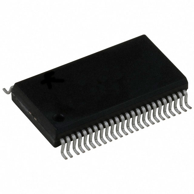
CDC857-3DGGR

Why Choose Us?
Professional Platform
B2B & B2C purchasingDelivery at full speed
1-2 days deliveryWide variety
Original manufacturers365 days guarantee
Responsible quality
.png)


Tech Specifications
CDC857-3DGGR Description
CDC857-3DGGR Description
The CDC857-3DGGR is a PLL Clock Driver IC designed by Texas Instruments, featuring a 48-TSSOP package and a 3.3V supply voltage. This component is specifically engineered for applications requiring precise clock distribution and synchronization. It operates within a temperature range of 0°C to 85°C, making it suitable for a variety of industrial and commercial environments. The CDC857-3DGGR supports a maximum frequency of 167MHz, ensuring high-performance clock distribution with minimal jitter.
CDC857-3DGGR Features
- PLL with Bypass Capability: The CDC857-3DGGR incorporates a Phase-Locked Loop (PLL) with bypass functionality, providing flexibility in clock generation and distribution. This feature allows the device to be used in both PLL-driven and direct clock input modes, enhancing its versatility.
- High Input/Output Differential Capability: The device supports differential signaling on both input and output, which reduces electromagnetic interference (EMI) and improves signal integrity. This is particularly beneficial in high-speed applications where signal quality is critical.
- Surface Mount Technology: The surface mount package type facilitates easy integration into modern PCB designs, ensuring reliable mechanical and electrical connections.
- Wide Supply Voltage Range: Operating within a 3V to 3.6V supply voltage range, the CDC857-3DGGR offers flexibility in power supply options, making it suitable for a wide range of applications.
- 1:10 Input to Output Ratio: This ratio allows for efficient clock distribution, multiplying the input clock signal to drive multiple output loads, which is ideal for systems requiring multiple synchronized clock signals.
- Obsolete Status: While the CDC857-3DGGR is marked as obsolete, it remains a reliable choice for legacy systems and applications where its specific features are still required.
- Compliance and Safety: The device is REACH unaffected and ROHS3 compliant, ensuring it meets environmental and safety standards, making it suitable for use in various industries.
CDC857-3DGGR Applications
The CDC857-3DGGR is ideal for applications that require precise clock distribution and synchronization. Its high-frequency capability and differential signaling make it particularly suitable for:
- Telecommunications Equipment: Providing stable clock signals for data transmission and synchronization in networking devices.
- High-Speed Data Converters: Ensuring accurate timing for ADCs and DACs in signal processing applications.
- Digital Signal Processing (DSP) Systems: Offering reliable clock distribution for DSPs and FPGAs in complex digital systems.
- Industrial Control Systems: Providing synchronized clock signals for PLCs and other industrial automation equipment.
- Test and Measurement Equipment: Ensuring precise timing for oscilloscopes, spectrum analyzers, and other test instruments.
Conclusion of CDC857-3DGGR
The CDC857-3DGGR from Texas Instruments is a robust PLL Clock Driver IC with a wide range of features that make it suitable for various high-performance applications. Its differential signaling capability, wide supply voltage range, and PLL with bypass functionality provide significant advantages over similar models. Despite its obsolete status, the CDC857-3DGGR remains a reliable choice for legacy systems and applications where its specific features are still required. Its compliance with environmental and safety standards ensures its suitability for use in diverse industries.
FAQ
| Quantity | Unit Price | Ext. Price |
|---|---|---|
| 61+ | $4.31200 | $263.03 |
Not available to buy online? Want the lower wholesale price? Please Send RFQ to get best price, we will respond immediately


.png?x-oss-process=image/format,webp/resize,h_32)


