

Texas Instruments
CDCL1810RGZRG4
Clock Buffers, Drivers ICs

Not available to buy online? Want the lower wholesale price? Please Send RFQ to get best price, we will respond immediately


.png?x-oss-process=image/format,webp/resize,p_30)


CDCL1810RGZRG4 Description
CDCL1810RGZRG4 Description
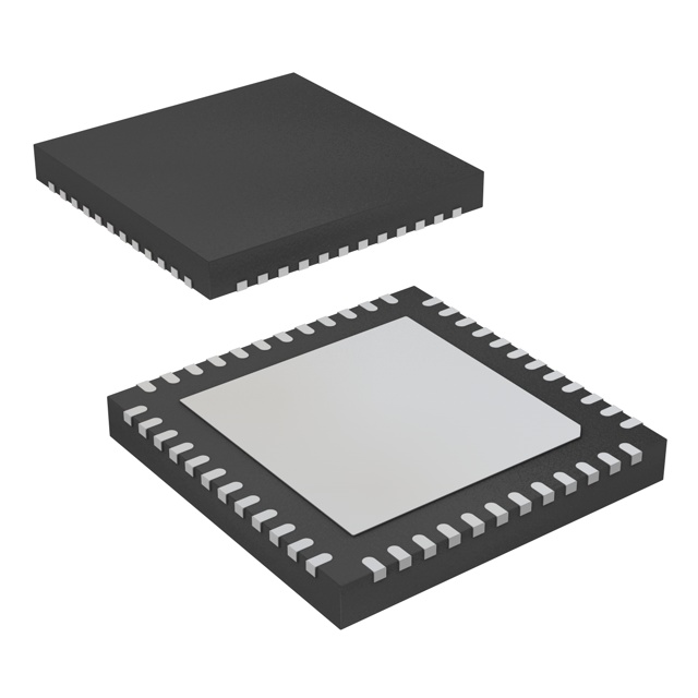
The CDCL1810RGZRG4 is a high-performance clock buffer designed by Texas Instruments, featuring a 1:10 input-to-output ratio and differential signaling on both the input and output stages. This fanout buffer is ideal for applications requiring precise clock distribution and signal integrity. The device operates within a supply voltage range of 1.7V to 1.9V and supports LVDS input and CML output, making it suitable for a wide range of high-speed applications. The CDCL1810RGZRG4 is packaged in a 48-pin VQFN format, ensuring robust mechanical and thermal performance. With a maximum operating frequency of 650 MHz, this IC is well-suited for demanding clock distribution tasks. The device is REACH unaffected and RoHS3 compliant, adhering to stringent environmental and safety standards. Its moisture sensitivity level is rated at MSL 3 (168 hours), ensuring reliability in various environmental conditions.
CDCL1810RGZRG4 Features
- High Input-to-Output Ratio: The 1:10 ratio allows for efficient distribution of clock signals, making it ideal for systems requiring multiple clock outputs from a single input.
- Differential Signaling: Both input and output stages support differential signaling, which enhances signal integrity and reduces electromagnetic interference (EMI).
- Wide Supply Voltage Range: Operating within 1.7V to 1.9V ensures compatibility with a variety of power supply configurations.
- High-Speed Performance: With a maximum operating frequency of 650 MHz, the CDCL1810RGZRG4 is capable of handling high-speed clock signals, making it suitable for advanced digital systems.
- Surface Mount Technology: The surface mount package type facilitates easy integration into modern PCB designs, enhancing reliability and reducing the risk of mechanical stress.
- Environmental Compliance: The device is REACH unaffected and RoHS3 compliant, ensuring it meets global environmental regulations and standards.
- Moisture Sensitivity Level: Rated at MSL 3 (168 hours), the CDCL1810RGZRG4 is designed to withstand various environmental conditions, ensuring long-term reliability.
CDCL1810RGZRG4 Applications
The CDCL1810RGZRG4 is well-suited for a variety of applications, including:
- Telecommunications: Ideal for high-speed data transmission systems, where precise clock distribution is critical for maintaining signal integrity.
- Networking Equipment: Used in routers, switches, and other networking devices to ensure reliable clock distribution across multiple components.
- High-Speed Computing: Suitable for server and workstation applications requiring high-frequency clock signals and efficient signal distribution.
- Industrial Automation: Provides robust clock distribution for industrial control systems, ensuring precise timing and synchronization.
- Consumer Electronics: Used in high-definition video processing and other consumer electronics applications where high-speed clock signals are required.
Conclusion of CDCL1810RGZRG4
The CDCL1810RGZRG4 from Texas Instruments is a versatile and high-performance clock buffer that offers significant advantages over similar models. Its 1:10 input-to-output ratio and differential signaling capabilities make it ideal for applications requiring precise clock distribution and signal integrity. The wide supply voltage range and high operating frequency ensure compatibility and performance in a variety of high-speed systems. With its surface mount package and environmental compliance, the CDCL1810RGZRG4 is a reliable choice for modern electronic designs. Whether in telecommunications, networking, computing, industrial automation, or consumer electronics, this device stands out for its performance, reliability, and versatility.
Tech Specifications
CDCL1810RGZRG4 Documents
Download datasheets and manufacturer documentation for CDCL1810RGZRG4
CDCL1810 Multiple Changes 02/Mar/2015 CDCL1810 Related Parts


Shopping Guide


.png?x-oss-process=image/format,webp/resize,h_32)


©2025 ERSA Electronics Corporation.