
Texas Instruments
CDCS501PW

Why Choose Us?
Professional Platform
B2B & B2C purchasingDelivery at full speed
1-2 days deliveryWide variety
Original manufacturers365 days guarantee
Responsible quality
.png)


Tech Specifications
CDCS501PW Description
CDCS501PW Description
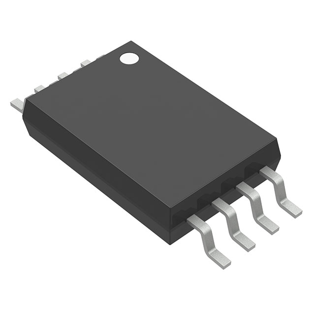
The CDCS501PW from Texas Instruments is a Spread Spectrum Clock Driver designed to provide precise clock signal distribution while minimizing electromagnetic interference (EMI). This surface-mount IC operates within a 3V to 3.6V supply range, making it suitable for low-power applications. With a maximum frequency of 108MHz, it supports LVCMOS input and output signals, ensuring compatibility with a wide range of digital systems. The device features a 1:1 input-to-output ratio and does not include PLL or divider/multiplier functionality, simplifying its integration into clock distribution networks. Packaged in an 8-pin TSSOP (Tube), it is RoHS3 compliant and REACH unaffected, meeting stringent environmental standards.
CDCS501PW Features
- Spread Spectrum Clocking: Reduces peak EMI emissions, improving system reliability in noise-sensitive environments.
- Low-Voltage Operation: 3V–3.6V supply range ensures compatibility with modern low-power designs.
- LVCMOS Interface: Supports single-ended LVCMOS input/output, simplifying signal integrity management.
- High Frequency Support: Up to 108MHz operation for demanding clock distribution applications.
- Compact & Reliable: 8-pin TSSOP package with MSL 1 (Unlimited) moisture sensitivity, ideal for automated assembly.
- Regulatory Compliance: RoHS3 and REACH compliant, ensuring adherence to global environmental standards.
CDCS501PW Applications
- Embedded Systems: Ideal for clock distribution in microcontrollers, FPGAs, and DSPs where EMI reduction is critical.
- Consumer Electronics: Used in smart devices, set-top boxes, and displays to mitigate clock-induced noise.
- Industrial Automation: Provides stable clock signals in PLCs, motor controllers, and sensor interfaces.
- Telecommunications: Ensures low-jitter clocking in networking equipment and data transmission systems.
- Medical Devices: Suitable for precision timing in diagnostic and monitoring equipment requiring EMI compliance.
Conclusion of CDCS501PW
The CDCS501PW is a robust, high-performance clock driver optimized for EMI-sensitive applications. Its spread spectrum capability, low-voltage operation, and compact form factor make it a versatile choice for modern electronic designs. With no PLL or frequency multiplication, it offers a straightforward solution for 1:1 clock distribution while meeting stringent environmental and regulatory standards. Engineers can leverage this device in consumer, industrial, and medical applications where signal integrity and EMI compliance are paramount.
FAQ
| Quantity | Unit Price | Ext. Price |
|---|---|---|
| 1+ | $1.35520 | $1.36 |
| 10+ | $0.98824 | $9.88 |
| 25+ | $0.89690 | $22.42 |
| 150+ | $0.77405 | $116.11 |
| 259+ | $1.02080 | $264.39 |
Not available to buy online? Want the lower wholesale price? Please Send RFQ to get best price, we will respond immediately


.png?x-oss-process=image/format,webp/resize,h_32)


