
 German
 Japanese
 Portuguese
 Korea
Korea
 Mexico
 Dutch
Dutch


Texas Instruments
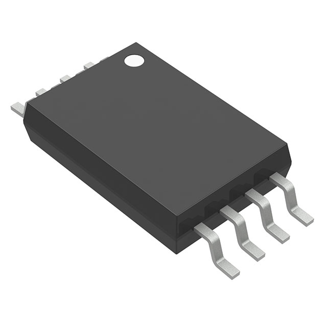
CDCS502PW

Why Choose Us?
Professional Platform
B2B & B2C purchasingDelivery at full speed
1-2 days deliveryWide variety
Original manufacturers365 days guarantee
Responsible quality
.png)


Tech Specifications
CDCS502PW Description
CDCS502PW Description
The CDCS502PW from Texas Instruments is a high-performance Spread Spectrum Clock Driver designed to reduce electromagnetic interference (EMI) in sensitive electronic systems. Operating within a 3V to 3.6V supply range, this IC delivers LVCMOS output signals with a maximum frequency of 108MHz, making it suitable for applications requiring precise clock distribution with minimized noise. The device features a 1:1 input-to-output ratio, accepts crystal input, and integrates a multiplier (no divider) to enhance signal integrity. Packaged in an 8-pin TSSOP and rated for surface-mount assembly, the CDCS502PW is RoHS3 compliant and adheres to REACH environmental standards, ensuring reliability in industrial and commercial environments.
CDCS502PW Features
- Spread Spectrum Clocking: Reduces peak EMI by modulating the clock frequency, improving compliance with regulatory standards.
- Low-Voltage Operation: Supports 3V–3.6V supplies, ideal for power-sensitive designs.
- High-Frequency Performance: Delivers stable outputs up to 108MHz with LVCMOS compatibility.
- Compact & Robust: 8TSSOP package with MSL1 (Unlimited) moisture sensitivity, suitable for automated PCB assembly.
- No PLL Required: Simplifies design by eliminating phase-locked loop complexity.
- Multiplier Function: Enables frequency multiplication without external components.
CDCS502PW Applications
- Embedded Systems: Clock distribution in microcontrollers, FPGAs, and DSPs.
- Communications Equipment: Reduces EMI in routers, switches, and baseband processors.
- Consumer Electronics: Ideal for TVs, set-top boxes, and audio/video interfaces requiring low-noise timing.
- Industrial Automation: Provides reliable clocking for sensors, motor controllers, and PLCs.
- Medical Devices: Ensures signal integrity in diagnostic and imaging equipment.
Conclusion of CDCS502PW
The CDCS502PW stands out as a versatile, EMI-optimized clock driver for modern electronic systems. Its spread spectrum capability, combined with high-frequency operation and a compact footprint, makes it a superior choice over fixed-frequency clock drivers. Engineers benefit from simplified integration, reduced BOM costs, and compliance with stringent environmental standards. Whether in consumer, industrial, or communication systems, this IC delivers precision and reliability while mitigating interference challenges.
FAQ
| Quantity | Unit Price | Ext. Price |
|---|---|---|
| 1+ | $2.73680 | $2.74 |
| 10+ | $2.04864 | $20.49 |
| 25+ | $1.87686 | $46.92 |
| 150+ | $1.64578 | $246.87 |
| 152+ | $1.74240 | $264.84 |
Not available to buy online? Want the lower wholesale price? Please Send RFQ to get best price, we will respond immediately


.png?x-oss-process=image/format,webp/resize,h_32)


