
 German
 Japanese
 Portuguese
 Korea
Korea
 Mexico
 Dutch
Dutch


Texas Instruments
CDCV855IPWR

Why Choose Us?
Professional Platform
B2B & B2C purchasingDelivery at full speed
1-2 days deliveryWide variety
Original manufacturers365 days guarantee
Responsible quality
.png)


Tech Specifications
CDCV855IPWR Description
CDCV855IPWR Description
The CDCV855IPWR is a high-performance PLL clock driver designed by Texas Instruments, suitable for a wide range of applications requiring precise clock management. This device features a phase-locked loop (PLL) with a bypass option, providing flexibility in clock generation and synchronization. The CDCV855IPWR operates within a supply voltage range of 2.3V to 2.7V and supports a maximum frequency of 180MHz, making it ideal for high-speed digital systems.
CDCV855IPWR Features
- PLL with Bypass Capability: The CDCV855IPWR includes a PLL that can be bypassed, offering enhanced flexibility in clock generation and synchronization. This feature allows designers to optimize performance based on specific application requirements.
- Wide Supply Voltage Range: The device operates within a supply voltage range of 2.3V to 2.7V, providing compatibility with various power supply configurations.
- High-Speed Performance: With a maximum frequency of 180MHz, the CDCV855IPWR is well-suited for high-speed digital systems, ensuring precise clock distribution and synchronization.
- Differential I/O: The CDCV855IPWR supports differential input and output, which enhances signal integrity and reduces electromagnetic interference (EMI).
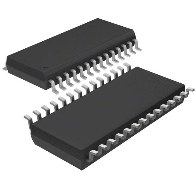
- Surface Mount Packaging: The device is available in a 28-TSSOP surface mount package, making it suitable for compact and high-density PCB designs.
- Compliance and Reliability: The CDCV855IPWR is REACH unaffected and RoHS3 compliant, ensuring environmental and regulatory standards are met. Additionally, it has a moisture sensitivity level (MSL) of 1, indicating unlimited storage time under specified conditions.
- Single Circuit Design: The device features a single circuit, simplifying design and reducing component count in clock distribution systems.
CDCV855IPWR Applications
The CDCV855IPWR is ideal for applications requiring high-speed clock distribution and synchronization, such as:
- High-Speed Digital Systems: The device's high-frequency capability and differential I/O make it suitable for systems requiring precise clock management, such as high-speed data converters and digital signal processors.
- Telecommunications: The CDCV855IPWR can be used in telecommunications equipment for clock synchronization and distribution, ensuring reliable and high-performance operation.
- Networking Equipment: In networking applications, the device can provide stable and synchronized clock signals for various components, improving overall system performance and reliability.
- Industrial Control Systems: The CDCV855IPWR's robust design and compliance with environmental and regulatory standards make it suitable for industrial control systems where reliability and precision are critical.
Conclusion of CDCV855IPWR
The CDCV855IPWR from Texas Instruments is a versatile PLL clock driver that offers high-speed performance, differential I/O, and flexible PLL operation. Its wide supply voltage range, surface mount packaging, and compliance with environmental and regulatory standards make it an ideal choice for a variety of applications. While it is not recommended for new designs, the CDCV855IPWR remains a reliable option for existing systems requiring precise clock management and synchronization.
FAQ
Not available to buy online? Want the lower wholesale price? Please Send RFQ to get best price, we will respond immediately


.png?x-oss-process=image/format,webp/resize,h_32)


