
 German
 Japanese
 Portuguese
 Korea
Korea
 Mexico
 Dutch
Dutch


Texas Instruments
CDCV857BDGG

Why Choose Us?
Professional Platform
B2B & B2C purchasingDelivery at full speed
1-2 days deliveryWide variety
Original manufacturers365 days guarantee
Responsible quality
.png)


Tech Specifications
CDCV857BDGG Description
CDCV857BDGG Description
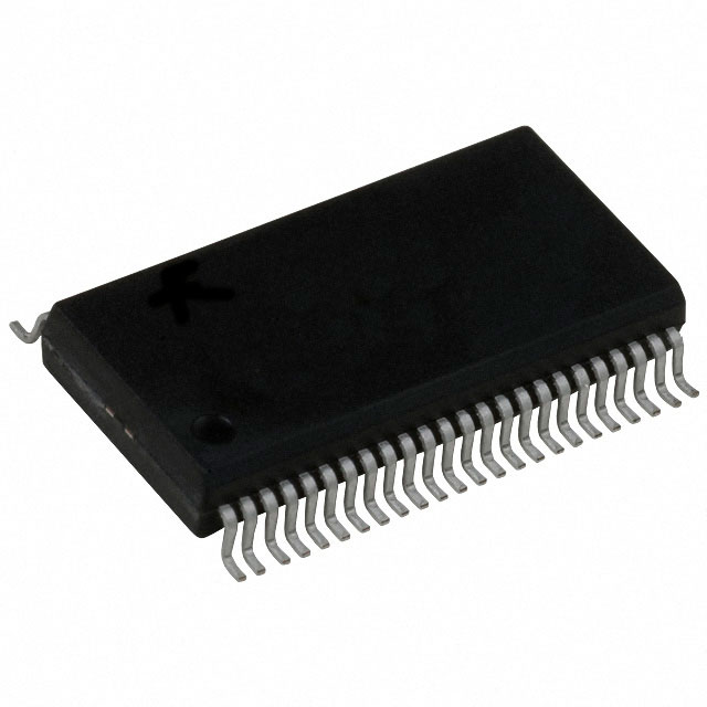
The CDCV857BDGG from Texas Instruments is a high-performance PLL-based clock driver designed for precision clock distribution in demanding electronic systems. Operating within a 2.3V to 2.7V supply range, this device supports frequencies up to 200MHz, making it suitable for high-speed applications. Housed in a 48-pin TSSOP package, it features a 1:10 input-to-output ratio with differential input and output capabilities, ensuring low-jitter signal integrity. The integrated PLL with bypass mode enhances flexibility, allowing seamless clock synchronization or direct signal routing.
CDCV857BDGG Features
- PLL with Bypass Mode: Enables low-jitter clock generation or direct signal pass-through for system flexibility.
- Differential I/O: Supports LVDS, LVPECL, or HCSL interfaces, reducing noise susceptibility in high-speed designs.
- Wide Frequency Range: Operates up to 200MHz, ideal for networking, telecom, and computing applications.
- Low Voltage Operation: 2.3V–2.7V supply range optimizes power efficiency in portable and embedded systems.
- Robust Packaging: 48-TSSOP surface-mount package ensures reliable performance in space-constrained layouts.
- Compliance: RoHS3 and REACH compliant, meeting global environmental standards.
CDCV857BDGG Applications
This clock driver excels in systems requiring high-fidelity clock distribution, such as:
- Networking Equipment: Synchronizes timing in switches, routers, and base stations.
- Data Centers: Ensures precise clocking for servers and storage arrays.
- Test & Measurement: Delivers stable signals for oscilloscopes and signal analyzers.
- FPGA/ASIC Systems: Provides low-skew clocks for multi-chip designs.
Conclusion of CDCV857BDGG
The CDCV857BDGG stands out for its PLL flexibility, differential signaling, and high-frequency support, making it a robust choice for clock distribution in mission-critical applications. While now obsolete, its design remains relevant for legacy systems requiring low-jitter, high-performance timing solutions. Engineers should evaluate alternative TI offerings for new designs but can rely on this device for proven performance in existing implementations.
FAQ
Not available to buy online? Want the lower wholesale price? Please Send RFQ to get best price, we will respond immediately


.png?x-oss-process=image/format,webp/resize,h_32)


