
Texas Instruments
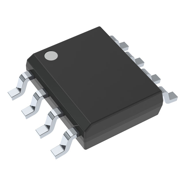
CDCVF2505DR
Clock Generators & Support Products


- 1+
- $1.46258
- $1.46
- 10+
- $1.34489
- $13.45
- 30+
- $1.27062
- $38.12
- 100+
- $1.19520
- $119.52
- 500+
- $1.16092
- $580.46
- 1000+
- $1.14607
- $1146.07

.png?x-oss-process=image/format,webp/resize,p_30)


CDCVF2505DR Description
CDCVF2505DR Description
The CDCVF2505DR is a high-performance PLL (Phase-Locked Loop) clock driver designed and manufactured by Texas Instruments. This device is part of the Clock Generators & Support Products category and is known for its ability to provide precise clock signals in various electronic systems. With a maximum frequency of 200MHz, this IC is suitable for applications requiring high-speed clock generation and distribution.
CDCVF2505DR Features
- PLL with Bypass: The CDCVF2505DR features a PLL that can be bypassed, providing flexibility in system design and operation.
- Input and Output Voltage: The device operates with an input and output voltage range of 3V to 3.6V, making it suitable for low-voltage applications.
- LVTTL Compatibility: Both the input and output are LVTTL compatible, ensuring compatibility with a wide range of digital systems.
- 1:5 Input to Output Ratio: The CDCVF2505DR can handle an input-to-output ratio of 1:5, allowing for efficient clock distribution.
- Surface Mount Technology: The device is designed for surface mount applications, making it ideal for space-constrained designs.
- REACH Unaffected and RoHS Compliant: The CDCVF2505DR is compliant with REACH regulations and RoHS standards, ensuring environmental and health safety.
- Moisture Sensitivity Level 1: With an MSL of 1, the device can be stored and handled without special precautions for moisture sensitivity.
CDCVF2505DR Applications
The CDCVF2505DR is ideal for a variety of applications where precise clock signals are required:
- High-Speed Data Communication: Due to its high-frequency capabilities, it is well-suited for applications such as Ethernet switches and routers.
- Telecommunications: The device can be used in telecom equipment for clock signal generation and distribution.
- Industrial Control Systems: Its reliability and performance make it suitable for use in industrial control systems where precise timing is critical.
- Consumer Electronics: In consumer electronics, such as set-top boxes and gaming consoles, the CDCVF2505DR can provide the necessary clock signals for high-speed data processing.
Conclusion of CDCVF2505DR
The CDCVF2505DR from Texas Instruments stands out due to its high-frequency capabilities, LVTTL compatibility, and flexible PLL with bypass feature. Its compliance with environmental standards and moisture sensitivity level make it a reliable choice for a wide range of applications. Whether used in high-speed data communication, telecommunications, industrial control systems, or consumer electronics, the CDCVF2505DR offers a robust solution for clock signal generation and distribution.
Tech Specifications
CDCVF2505DR Documents
Download datasheets and manufacturer documentation for CDCVF2505DR
 Wafer Fab Site 21/May/2019
  CDCVF2505
  CDCVF2505
  Design 25/Feb/2022
 Shopping Guide


.png?x-oss-process=image/format,webp/resize,h_32)


