
Texas Instruments
TLV9352QPWRQ1
OP Amps, Buffer Amps ICs


.png?x-oss-process=image/format,webp/resize,p_30)


TLV9352QPWRQ1 Description
TLV9352QPWRQ1 Description
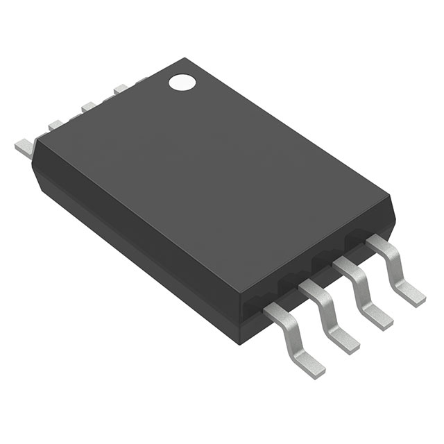
The TLV9352QPWRQ1 is a high-performance, dual-channel operational amplifier (op-amp) designed for automotive applications. Manufactured by Texas Instruments, this IC is optimized for surface-mount technology and is available in a tape and reel package, making it suitable automated for assembly processes. The TLV9352QPWRQ1 features a wide supply voltage range, from a minimum of 4.5 V to a maximum of 40 V, ensuring compatibility with various power supply configurations.
TLV9352QPWRQ1 Features
- Wide Supply Voltage Range: The TLV9352QPWRQ1 operates within a supply voltage span of 4.5 V to 40 V, providing flexibility for different power supply requirements.
- High Slew Rate: With a slew rate of 20 V/µs, the amplifier can handle high-frequency signals efficiently, making it suitable for applications requiring fast transient response.
- Gain Bandwidth Product: The 3.5 MHz gain bandwidth product ensures that the TLV9352QPWRQ1 can maintain high gain at higher frequencies, ideal for signal processing and filtering applications.
- Low Supply Current: Each channel of the TLV9352QPWRQ1 consumes only 650 µA, contributing to energy efficiency and reduced power consumption.
- Low Input Bias Current: The 10 pA input bias current minimizes the impact of input currents on the signal, resulting in higher accuracy and stability.
- Low Input Offset Voltage: The 350 µV input offset voltage ensures minimal error in the output signal, enhancing the precision of the amplifier.
- High Output Current: Each channel can deliver up to 60 mA of output current, making the TLV9352QPWRQ1 capable of driving moderate to high load applications.
- Automotive Grade: The TLV9352QPWRQ1 is designed to meet the stringent requirements of the automotive industry, ensuring reliability and robustness in harsh environments.
TLV9352QPWRQ1 Applications
The TLV9352QPWRQ1 is well-suited for a variety of automotive applications due to its robust design and high performance. Specific use cases include:
- Automotive Electronics: Ideal for automotive control units, infotainment systems, and sensor interfaces where high reliability and performance are critical.
- Signal Conditioning: The TLV9352QPWRQ1 can be used for amplifying and conditioning signals from various sensors, such as temperature, pressure, and position sensors.
-Power ** Management**: The low supply current and high output current capabilities make it suitable for power management circuits in automotive systems. - Audio Applications: The high slew rate and gain bandwidth product make it suitable for audio amplifiers and preamplifiers in automotive audio systems.
Conclusion of TLV9352QPWRQ1
The TLV9352QPWRQ1 from Texas Instruments is a versatile and high-performance dual-channel op-amp designed specifically for automotive applications. Its wide supply voltage range, high slew rate, and low supply current make it ideal an choice for a variety of automotive electronics, signal conditioning, and power management applications. The automotive grade reliability ensures that it can withstand the harsh conditions often encountered in automotive environments. Overall, the TLV9352QPWRQ1 offers a compelling combination of performance, efficiency, and robustness, making it a standout choice for engineers designing automotive systems.
Tech Specifications
TLV9352QPWRQ1 Documents
Download datasheets and manufacturer documentation for TLV9352QPWRQ1
 TLV935x-Q1
 Shopping Guide


.png?x-oss-process=image/format,webp/resize,h_32)


