

Transistor MTL2N2222AUB — The Playful, Practical, Pin‑Sharp Guide

If the 2N2222 is the MCU‑world’s friendly neighborhood superhero, then transistor MTL2N2222AUB is its high‑reliability, hermetically sealed, mission‑ready alter‑ego. Same classic moves, tougher costume: a ceramic UB chip‑carrier built for demanding environments from lab racks to launch pads.
NPN small‑signal BJT (2N2222A family)
~50 V (family typical)
Up to ~0.8 A (pulsed limits apply)
UB ceramic, hermetic, 3‑pin
1) Meet transistor MTL2N2222AUB
Think of the 2N2222A as the MCU cameo in almost every electronics origin story. Now give it a Dune‑grade stillsuit and a Top Gun flight check: that’s transistor MTL2N2222AUB. It’s a general‑purpose NPN BJT with the familiar 2N2222A electrical personality, but housed in a hermetically sealed ceramic UB package for long‑life, high‑temperature, and high‑reliability use. Many vendors list the same silicon under part strings like 2N2222AUB, MNS2N2222AUB, or MSR2N2222AUB depending on screening level and supply chain; engineers often shorthand all of these as “UB 2N2222A.”
2) Quick spec sheet — what matters in practice
| Parameter | Typical value | Why you care |
|---|---|---|
| VCEO | 50 V | Room to switch 24 V rails with plenty of margin. |
| VCBO | 75 V | Protects against flyback spikes with proper clamps. |
| IC (cont) | 800 mA | Comfortable for relays, solenoids, small motors (pulsed higher). |
| PD | 0.3 W @ 25 °C (1.0 W @ TC=25 °C) | Derate smartly; ceramic helps at case‑cooled. |
| hFE | 100 @ 10 mA; 30 @ 500 mA | Design base drive with headroom; avoid skimping at high Ic. |
| VCE(sat) | 0.3 V @ 150 mA | Low loss for low‑side switches and level shifting. |
| ton/toff | 35 ns / 300 ns | Snappy for kHz‑MHz digital & RF small‑signal stages. |
| TJ | −65 … +200 °C | Wide mission profile with hermetic seal. |
Values representative of the 2N2222AUB family; check your exact lot sheet for limits and screening.
- transistor MTL2N2222AUB keeps the familiar 2N2222A behavior but with improved reliability.
- Great for sensor interfaces, transistor arrays, level shifters, and RF buffer stages.
- Pairs nicely with logic‑level MOSFET gates as a pre‑driver or clamp.
.png?x-oss-process=image/auto-orient,1/quality,q_70/format,webp)
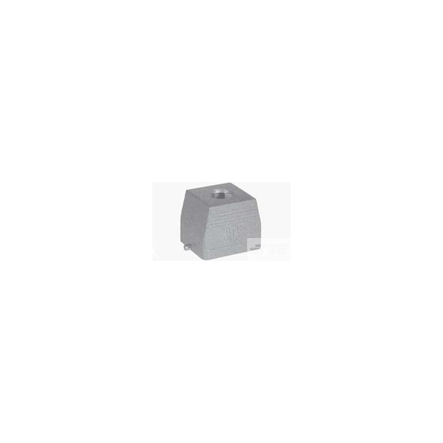
3) UB ceramic package: pins, dimensions & footprints
Pinout (viewed from top)
- Pad 1 = Base
- Pad 2 = Emitter
- Pad 3 = Collector
- Optional Pad 4 on some lids is a shield tied to the lid.
Orientation key is notched; castellations run through the ceramic for robust solder fillets.
Typical UB dimensions (inches — mm for reference)
| Symbol | Min (in) | Max (in) | Min (mm) | Max (mm) | Notes |
|---|---|---|---|---|---|
| CH | .061 | .075 | 1.55 | 1.90 | Overall package thickness; window lid adds .010–.040 in. |
| BL | .215 | .225 | 5.46 | 5.71 | Body length (example UB drawing) |
| BW | .145 | .155 | 3.68 | 3.93 | Body width |
| LW | .022 | .028 | 0.56 | 0.71 | Castellation width |
| LW2 | .006 | .022 | 0.15 | 0.56 | Castellation throat min/max (unobstructed) |
| L3 | .003 | .007 | 0.08 | 0.18 | Castellation depth |
| LL1 | .032 | .048 | 0.81 | 1.22 | Lead/land length, bottom layer |
| LL2 | .072 | .088 | 1.83 | 2.23 | Lead/land length, mid layer |
| LS | .045 | .055 | 1.14 | 1.39 | Seating span |
Dimensions are typical for UB carriers; verify against the vendor drawing delivered with your transistor MTL2N2222AUB lot. Millimeters are informational.
4) When to choose transistor MTL2N2222AUB over other 2N2222 variants
- Reliability & environment: you need hermetic sealing, wider temperature, or MIL‑style screening for aerospace/defense/industrial.
- Parasitics matter: UB’s compact geometry can be cleaner than TO‑18/TO‑92 in RF or fast switching.
- PCB assembly: surface‑mount reflow with robust solder fillets on castellations.
- Form‑fit control: you want footprint stability and good coplanarity for automated AOI/X‑ray.
.png?x-oss-process=image/auto-orient,1/quality,q_70/format,webp)
5) Design‑in checklist
Bias for saturation switching
Target Ic: 300 mA
Choose Ib ≈ Ic/10 → 30 mA (ensure base driver can source)
Check VCE(sat) @ 150–300 mA, add margin.
Clamp flyback with Schottky/TVS; keep VCES safe.
Small‑signal gain stages
Set collector load RC for desired swing.
Choose RE for bias stability (1–10 kΩ range typical).
Aim for collector ≈ VCC/2 at quiescent; use emitter bypass cap for gain.
Speed tips
- Use a small base‑emitter resistor (22–100 kΩ) to hasten turn‑off.
- Add a base series resistor to tame ringing and limit base current.
- For MHz use, minimize pad/trace capacitance; UB helps.
Thermals
- Free‑air PD ~0.3 W at 25 °C; derate ~6.6 mW/°C above 25 °C.
- Case‑cooled PD can hit ~1.0 W with copper under‑pad and airflow.
EMC & ESD
- Put TVS where cables enter; add RC snubbers across inductive loads.
- Kelvin your sense resistors; keep dv/dt nodes orthogonal to B/E pads.
Quality hooks
- Log lot/batch IDs; archive X‑ray and AOI shots of the UB solder fillets.
- Store calibration/drive coefficients in firmware for traceability.
6) PCB, footprint & reliability notes
- Footprint: keep pads slightly wider than LW to promote toe fillets; solder mask defined pads help repeatability.
- Co‑planarity: spec ≤0.006 in (0.15 mm) max deviation for leadless carriers; verify on incoming inspection.
- Standoff: respect seating plane; avoid tombstoning with symmetric paste apertures.
- Conformal coat: UB is hermetic but board is not — coat for condensation/altitude if needed.
.png?x-oss-process=image/auto-orient,1/quality,q_70/format,webp)
7) SPICE model & test benches
You can drop a generic 2N2222A model and tighten it with measured hFE, Cibo, and VCE(sat) from your transistor MTL2N2222AUB lot card. Two handy benches:
Switching loss probe
• Drive: 0–5 V step through 330 Ω base resistor
• Load: 200 mA inductive, 12 V, Schottky clamp
• Metrics: t_on, t_off, Q_base, VCE(sat)
Small‑signal gain probe
• Bias: VCC=12 V, RC=3.3 k, RE=1 k, Vin=10 mV AC
• Sweep: 100 Hz to 10 MHz, extract mid‑band gain & pole
8) Application playbook — eight mini‑designs
A. Logic‑to‑relay low‑side
GPIO → 1k → Base | Emitter→GND | Collector→Relay−
Relay+→12 V | Diode across coil | Base‑emitter 100 kΩ
For 12 V, 200 mA coils, budget 20–30 mA base current for crisp saturation.
B. MOSFET gate clamp/driver
Use transistor MTL2N2222AUB as a level‑shifted pre‑driver to discharge gates quickly in push‑pull totem poles.
C. Sensor current buffer
Active‑collector follower for 4–20 mA loops, with VCE headroom and thermal derating.
D. RF pre‑buffer
UB’s compact parasitics make an excellent 100 MHz pre‑buffer for ham‑band experiments.
E. PWM solenoid driver
At 1–5 kHz PWM, keep the base impedance low and clamp with Schottky + TVS to control emission.
F. Audio metering LED
Use as a log‑amp stage with emitter degeneration for level meters.
G. LDO bypass switch
Turn on a measurement rail briefly; PD limit rules apply.
H. Watchdog beeper
Drive small buzzers directly up to tens of mA with headroom to spare.
.png?x-oss-process=image/auto-orient,1/quality,q_70/format,webp)
9) Production test & screening notes
- Screen per your vendor’s MIL profile (e.g., burn‑in at VCB=30 V, typical 80 h) and temperature extremes.
- Sample hFE bins at multiple IC points; store lot stats for corner analysis.
- Inspect castellations for full wetting; X‑ray optional, AOI recommended.
10) Cross‑references & cousins
- 2N2222AUB / transistor MTL2N2222AUB — ceramic UB, hermetic, SMD.
- MNS2N2222AUB / MSR2N2222AUB — similar silicon with different screening levels.
- P2N2222A / TO‑92 / TO‑18 — plastic/metal can variants if cost/availability dominates.
Always confirm voltage, current, and hFE bins in the specific datasheet before swapping.
11) FAQ
Is transistor MTL2N2222AUB drop‑in for a plastic SOT‑23 2N2222A?
Electrically similar, yes; mechanically different footprint. UB’s parasitics and thermal behavior can be better at RF and under case‑cooled conditions.
What’s the safe base drive rule?
For switching, design IB ≈ IC/10 and verify VCE(sat) at the intended current; then optimize downwards if margins look good.
How hot is too hot?
Stay within the package PD and junction range; derate above 25 °C and consider copper pour under the UB body for heat spreading.
12) Work with ERSA Electronics
ERSA stocks transistor MTL2N2222AUB family devices and functionally equivalent 2N2222AUB options with fast sampling. Need cross‑references, screening paperwork, or X‑ray/lot traceability? We’ve got you.
- Hermetic UB 2N2222A variants (TX/TXV/space‑grade on request)
- Footprint, pick‑and‑place, paste aperture suggestions
- Reference designs and BOM alternates to secure supply
Appendix — Legacy metal‑can notes (for reference)
Many historical drawings list TO‑18/TO‑39 style dimensions and gauge‑plane rules. Typical values seen in public resources include:
| Symbol | Min (in) | Max (in) | Min (mm) | Max (mm) | Notes |
|---|---|---|---|---|---|
| CD | .178 | .195 | 4.52 | 4.95 | Body diameter |
| CH | .170 | .210 | 4.32 | 5.33 | Can height |
| HD | .209 | .230 | 5.31 | 5.84 | Header diameter |
| LD | .016 | .021 | 0.41 | 0.53 | Lead diameter |
| LL | .500 | .750 | 12.70 | 19.05 | Lead length; L‑suffix devices: 1.5–1.75 in |
| LU | .016 | .019 | 0.41 | 0.48 | Lead undercut |
| L1 | .050 | — | 1.27 | — | Gauge features |
| L2 | .250 | — | 6.35 | — | Gauge features |
| P | .100 | — | 2.54 | — | Lead pitch |
| Q | .030 | — | 0.76 | — | Tab dimension |
| TL | .028 | .048 | 0.71 | 1.22 | Tab length (see header notes) |
| TW | .036 | .046 | 0.91 | 1.17 | Tab width |
| r | .010 | — | 0.25 | — | Inside corner radius |
Use these only when comparing with legacy drawings; UB is the focus for transistor MTL2N2222AUB.

Related Articles
- ·MOSFET Transistor — The Practical, No-Drama Switch That Powers Modern Electronics
- ·MOSFET vs BJT Transistor — A Fun, Field‑Ready, No‑Nonsense Guide
- ·Transistor MTL2N2222AUB — The Playful, Practical, Pin‑Sharp Guide
- ·2N2222 Transistor: The Tiny Switch-Star That Still Steals the Scene
- ·Darlington Transistor: Big Gain, Bigger Personality
- ·BC547 Transistor: The Tiny NPN That Stars in a Billion Circuits
- ·NPN vs PNP Transistor: A Cinematic Showdown for Real-World Circuits
- ·Insulated Gate Bipolar Transistor (IGBT): The Dragon Rider of High-Power Circuits
- ·Transistor Symbol: The Blockbuster Guide (With Zero Boring)
- ·NMOS Transistor: The Silicon Speedster Powering 2025's Tech🚀


.png?x-oss-process=image/format,webp/resize,h_32)


