

Not available to buy online? Want the lower wholesale price? Please Send RFQ to get best price, we will respond immediately


.png?x-oss-process=image/format,webp/resize,p_30)


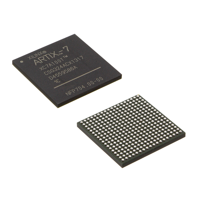
XC7A15T-1CSG324I Description
XC7A15T-1CSG324I Overview
FPGA chips are designed with 210 I/Os to allow for more organized data transport. A basic building block has 16640 logic cells or components. The power source is a 1V-volt supply. The development board can be connected to this FPGA module via Surface Mount connections. The device needs a supply voltage between 0.95 and 1.05 volts to function. A temperature between -40°C and 100°C TJ must be maintained at all times to guarantee a safe and effective operation. This FPGA model is packed within Tray as a space-saving technique.
XC7A15T-1CSG324I Features
Endpoint and Root Port designs
Wide variety of configuration options, including support for commodity memories, 256-bit AES encryption with HMAC/SHA-256 authentication, and built-in SEU detection and correction.
Low-cost, wire-bond, bare-die flip-chip, and high signal integrity flip-chip packaging offer easy migration between family members in the same package. All packages are available in Pb-free and selected packages in the Pb option.
XC7A15T-1CSG324I Applications
Artificial Intelligence
5G Technology
Cloud Computing
Wireless Technology
Industrial Control
Tech Specifications
XC7A15T-1CSG324I Documents
Download datasheets and manufacturer documentation for XC7A15T-1CSG324I
 7 Series FPGA Overview 7 Series FPGAs PCB Design Guide Artix-7 FPGAs Datasheet Xilinx REACH211 Cert Xiliinx RoHS Cert
 Related Parts


Relevant Search
Shopping Guide


.png?x-oss-process=image/format,webp/resize,h_32)


©2025 ERSA Electronics Corporation.